Co-reporter:Mohammad Aghazadeh Meshgi, Subhajit Biswas, David McNulty, Colm O’Dwyer, Giuseppe Alessio Verni, John O’Connell, Fionán Davitt, Ilse Letofsky-Papst, Peter Poelt, Justin D. Holmes, and Christoph Marschner
Chemistry of Materials May 23, 2017 Volume 29(Issue 10) pp:4351-4351
Publication Date(Web):May 8, 2017
DOI:10.1021/acs.chemmater.7b00714
New oligosilylgermane compounds with weak Ge–H bonds have been used as precursors for the rapid synthesis of germanium (Ge) nanowires in high yields (>80%), via a solution–liquid–solid (SLS) mechanism, using indium (In) nanoparticles as a seeding agent over a temperature range between 180 and 380 °C. Even at low growth temperatures, milligram quantities of Ge nanowires could be synthesized over a reaction period of between 5 and 10 min. The speed of release of Ge(0) into the reaction environment can be tuned by altering the precursor type, synthesis temperature, and the presence or lack of an oxidizing agent, such as tri-n-octylphosphine oxide (TOPO). Energy-dispersive X-ray analysis showed that silicon atoms from the precursors were not incorporated into the structure of the Ge nanowires. As both In and Ge facilitate reversible alloying with Li, Li-ion battery anodes fabricated with these nanowires cycled efficiently with specific capacities, i.e., >1000 mAh g–1
Co-reporter:John O’Connell, Enrico Napolitani, Giuliana Impellizzeri, Colm Glynn, Gerard P. McGlacken, Colm O’Dwyer, Ray Duffy, and Justin D. Holmes
ACS Omega May 2017? Volume 2(Issue 5) pp:1750-1750
Publication Date(Web):May 1, 2017
DOI:10.1021/acsomega.7b00204
The functionalization and subsequent monolayer doping of InGaAs substrates using a tin-containing molecule and a compound containing both silicon and sulfur was investigated. Epitaxial InGaAs layers were grown on semi-insulating InP wafers and functionalized with both sulfur and silicon using mercaptopropyltriethoxysilane and with tin using allyltributylstannane. The functionalized surfaces were characterized using X-ray photoelectron spectroscopy (XPS). The surfaces were capped and subjected to rapid thermal annealing to cause in-diffusion of dopant atoms. Dopant diffusion was monitored using secondary ion mass spectrometry. Raman scattering was utilized to nondestructively determine the presence of dopant atoms, prior to destructive analysis, by comparison to a blank undoped sample. Additionally, due to the As-dominant surface chemistry, the resistance of the functionalized surfaces to oxidation in ambient conditions over periods of 24 h and 1 week was elucidated using XPS by monitoring the As 3d core level for the presence of oxide components.
Co-reporter:John O’Connell, Gillian Collins, Gerard P. McGlacken, Ray Duffy, and Justin D. Holmes
ACS Applied Materials & Interfaces 2016 Volume 8(Issue 6) pp:4101
Publication Date(Web):January 26, 2016
DOI:10.1021/acsami.5b11731
In this article, the functionalization of planar silicon with arsenic- and phosphorus-based azides was investigated. Covalently bonded and well-ordered alkyne-terminated monolayers were prepared from a range of commercially available dialkyne precursors using a well-known thermal hydrosilylation mechanism to form an acetylene-terminated monolayer. The terminal acetylene moieties were further functionalized through the application of copper-catalyzed azide–alkyne cycloaddition (CuAAC) reactions between dopant-containing azides and the terminal acetylene groups. The introduction of dopant molecules via this method does not require harsh conditions typically employed in traditional monolayer doping approaches, enabling greater surface coverage with improved resistance toward reoxidation. X-ray photoelectron spectroscopy studies showed successful dialkyne incorporation with minimal Si surface oxidation, and monitoring of the C 1s and N 1s core-level spectra showed successful azide–alkyne cycloaddition. Electrochemical capacitance–voltage measurements showed effective diffusion of the activated dopant atoms into the Si substrates.Keywords: alkyne−azide cycloaddition; arsenic; click chemistry; doping; functionalization; monolayer; phosphorus; silicon;
Co-reporter:Subhajit Biswas, Jessica Doherty, Dipanwita Majumdar, Tandra Ghoshal, Kamil Rahme, Michelle Conroy, Achintya Singha, Michael A. Morris, and Justin D. Holmes
Chemistry of Materials 2015 Volume 27(Issue 9) pp:3408
Publication Date(Web):April 16, 2015
DOI:10.1021/acs.chemmater.5b00697
One-dimensional nanostructures with controllable morphologies and defects are appealing for use in nanowire devices. This paper details the influence of colloidal magnetite iron oxide nanoparticle seeds to regulate the radial dimension and twin boundary formation in Ge nanowires grown through a liquid-injection chemical vapor deposition process. Control over the mean nanowire diameter, even in the sub-10 nm regime, was achieved due to the minimal expansion and aggregation of iron oxide nanoparticles during the growth process. The uncommon occurrence of heterogeneously distributed multiple layer {111} twins, directed perpendicular to the nanowire growth axis, were also observed in ⟨111⟩-directed Ge nanowires, especially those synthesized from patterned hemispherical Fe3O4 nanodot catalysts. Consecutive twin planes along ⟨111⟩-oriented nanowires resulted in a local phase transformation from 3C diamond cubic to hexagonal 4H allotrope. Localized polytypic crystal phase heretostructures were formed along ⟨111⟩-oriented Ge nanowire using magnetite nanodot catalysts.
Co-reporter:John O’Connell, Giuseppe Alessio Verni, Anushka Gangnaik, Maryam Shayesteh, Brenda Long, Yordan M. Georgiev, Nikolay Petkov, Gerard P. McGlacken, Michael A. Morris, Ray Duffy, and Justin D. Holmes
ACS Applied Materials & Interfaces 2015 Volume 7(Issue 28) pp:15514
Publication Date(Web):June 26, 2015
DOI:10.1021/acsami.5b03768
This article describes for the first time the controlled monolayer doping (MLD) of bulk and nanostructured crystalline silicon with As at concentrations approaching 2 × 10²⁰ atoms cm–3. Characterization of doped structures after the MLD process confirmed that they remained defect- and damage-free, with no indication of increased roughness or a change in morphology. Electrical characterization of the doped substrates and nanowire test structures allowed determination of resistivity, sheet resistance, and active doping levels. Extremely high As-doped Si substrates and nanowire devices could be obtained and controlled using specific capping and annealing steps. Significantly, the As-doped nanowires exhibited resistances several orders of magnitude lower than the predoped materials.Keywords: abrupt; arsenic; doping; high carrier concentration; MLD; monolayer; shallow;
Co-reporter:Colm O'Regan, Subhajit Biswas, Sven Barth, Michael A. Morris, Nikolay Petkov and Justin D. Holmes
Journal of Materials Chemistry A 2014 vol. 2(Issue 23) pp:4597-4605
Publication Date(Web):18 Apr 2014
DOI:10.1039/C4TC00136B
We report the size-controlled growth of Ge nanowires from Au–Ag–Ge ternary alloy catalysts. Significantly, Au–Ag–Ge layered thin films enabled, for the first time, the synthesis of high aspect ratio Ge nanowires by simultaneously manipulating both the solute concentration (C) and equilibrium concentration (Ceq.) of Ge in the catalysts, thereby increasing the Ge supersaturation during vapour–liquid–solid (VLS) growth. Simultaneous manipulation of C and Ceq. to enhance nanowire growth rates was also achieved using colloidal Au0.75–Ag0.25 nanoparticles deposited on a Ge film. These nanoparticles produced Ge nanowires with more uniform diameter distributions than those obtained from the thin films. The manifestation of the Gibbs–Thomson effect, resulting in a diameter dependent growth rate, was observed for all nanowires grown from Au0.75–Ag0.25 nanoparticles. In situ TEM heating experiments performed on the as-grown Ge nanowires enabled direct determination of the Ge equilibrium concentrations in the Au–Ag–Ge ternary alloys.
Co-reporter:Colm O'Regan, Subhajit Biswas, Nikolay Petkov and Justin D. Holmes
Journal of Materials Chemistry A 2014 vol. 2(Issue 1) pp:14-33
Publication Date(Web):11 Oct 2013
DOI:10.1039/C3TC31736F
One-dimensional semiconductor nanostructures have been studied in great depth over the past number of decades as potential building blocks in electronic, thermoelectric, optoelectronic, photovoltaic and battery devices. Silicon has been the material of choice in several industries, in particular the semiconductor industry, for the last few decades due to its stable oxide and well documented properties. Recently however, Ge has been proposed as a candidate to replace Si in microelectronic devices due to its high charge carrier mobilities. A number of various ‘bottom-up’ synthetic methodologies have been employed to grow Ge nanowires, including chemical vapour deposition, thermal evaporation, template methods, supercritical fluid synthesis, molecular beam epitaxy and solution phase synthesis. These bottom-up methods afford the opportunity to produce commercial scale quantities of nanowires with controllable lengths, diameters and crystal structure. An understanding of the vapour–liquid–solid (VLS) and vapour–solid–solid (VSS) mechanism by which most Ge nanowires are produced, is key to controlling their growth rate, aspect ratio and morphology. This article highlights the various bottom-up growth methods that have been used to synthesise Ge nanowires over the past 5–6 years, with particular emphasis on the Au/Ge eutectic system and the VLS mechanism. Thermodynamic and kinetic models used to describe Ge nanowire growth and morphology control will also be discussed in detail.
Co-reporter:Gillian Collins ; Michael Schmidt ; Gerard P. McGlacken ; Colm O’Dwyer
The Journal of Physical Chemistry C 2014 Volume 118(Issue 12) pp:6522-6530
Publication Date(Web):March 6, 2014
DOI:10.1021/jp500716z
A critical aspect in the practical applications and catalytic performance of shape-controlled nanocrystals is their stability and morphology retention under ambient conditions. Changes to the morphology of shape-controlled Pd nanocrystals capped by PVP are assessed by TEM, and surface oxidation was evaluated by X-ray photoelectron spectroscopy (XPS) over 12 months. Surface oxidation of PVP-capped Pd nanocrystals resulted in the loss of edge and corner sites and a transition to spherical morphologies. The shape stability of the nanocrystals was found to follow the trend cubic < cuboctahedra < octahedral ∼ concave cubes. For low index planes, {111} surfaces were more resistant to oxidation compared to {100} facets, correlating with the surface free energy of the nanocrystals. Cubic and cuboctahedral nanocrystals transitioned to spherical particles while octahedral nanocrystals retained their morphology. The presence of high-energy {110} facets was observed in the cubic nanocrystals which undergo surface reconstruction. The presence of surface defects may also influence the rate of the structural changes. Concave cubic nanocrystals, which possess high index facets and surface energies, were consistently found to display excellent morphology retention. The concave cubic nanocrystals displayed superior shape stability and reduced oxidation compared to cubic and cuboctahedral nanocrystals. XPS analysis further determined that PVP capping ligands on different Pd surface facets strongly influenced the morphological consistency. The stability of the concave cubes can be attributed to the stronger chemisorption of PVP capping ligands to the high index planes, making them less susceptible to oxidation.
Co-reporter:Mark J. Armstrong;Colm O’Dwyer;William J. Macklin;Justin. D. Holmes
Nano Research 2014 Volume 7( Issue 1) pp:1-62
Publication Date(Web):2014 January
DOI:10.1007/s12274-013-0375-x
The performance of the lithium-ion cell is heavily dependent on the ability of the host electrodes to accommodate and release Li+ ions from the local structure. While the choice of electrode materials may define parameters such as cell potential and capacity, the process of intercalation may be physically limited by the rate of solid-state Li+ diffusion. Increased diffusion rates in lithium-ion electrodes may be achieved through a reduction in the diffusion path, accomplished by a scaling of the respective electrode dimensions. In addition, some electrodes may undergo large volume changes associated with charging and discharging, the strain of which, may be better accommodated through nanostructuring. Failure of the host to accommodate such volume changes may lead to pulverisation of the local structure and a rapid loss of capacity. In this review article, we seek to highlight a number of significant gains in the development of nanostructured lithium-ion battery architectures (both anode and cathode), as drivers of potential next-generation electrochemical energy storage devices.
Co-reporter:Dr. Gillian Collins;Michael Schmidt;Dr. Colm O'Dwyer; Justin D. Holmes;Dr. Gerard P. McGlacken
Angewandte Chemie International Edition 2014 Volume 53( Issue 16) pp:4142-4145
Publication Date(Web):
DOI:10.1002/anie.201400483
Abstract
The shape sensitivity of Pd catalysts in Suzuki–Miyaura coupling reactions is studied using nanocrystals enclosed by well-defined surface facets. The catalytic performance of Pd nanocrystals with cubic, cuboctahedral and octahedral morphologies are compared. Superior catalytic reactivity is observed for Pd NCs with {100} surface facets compared to {111} facets. The origin of the enhanced reactivity associated with a cubic morphology is related to the leaching susceptibility of the nanocrystals. Molecular oxygen plays a key role in facilitating the leaching of Pd atoms from the surface of the nanocrystals. The interaction of O2 with Pd is itself facet-dependent, which in turn gives rise to more efficient leaching from {100} facets, compared to {111} facets under the reaction conditions.
Co-reporter:Dr. Gillian Collins;Michael Schmidt;Dr. Colm O'Dwyer; Justin D. Holmes;Dr. Gerard P. McGlacken
Angewandte Chemie 2014 Volume 126( Issue 16) pp:4226-4229
Publication Date(Web):
DOI:10.1002/ange.201400483
Abstract
The shape sensitivity of Pd catalysts in Suzuki–Miyaura coupling reactions is studied using nanocrystals enclosed by well-defined surface facets. The catalytic performance of Pd nanocrystals with cubic, cuboctahedral and octahedral morphologies are compared. Superior catalytic reactivity is observed for Pd NCs with {100} surface facets compared to {111} facets. The origin of the enhanced reactivity associated with a cubic morphology is related to the leaching susceptibility of the nanocrystals. Molecular oxygen plays a key role in facilitating the leaching of Pd atoms from the surface of the nanocrystals. The interaction of O2 with Pd is itself facet-dependent, which in turn gives rise to more efficient leaching from {100} facets, compared to {111} facets under the reaction conditions.
Co-reporter:Subhajit Biswas, Colm O’Regan, Nikolay Petkov, Michael A. Morris, and Justin D. Holmes
Nano Letters 2013 Volume 13(Issue 9) pp:4044-4052
Publication Date(Web):August 6, 2013
DOI:10.1021/nl401250x
This article describes an innovative approach in which bimetallic alloy seeds of AuxAg1–x are used to enhance the growth kinetics of Ge nanowires, via a vapor–liquid–solid (VLS) growth technique. The decreased equilibrium concentration and increased supersaturation of Ge in the liquid alloy seeds, compared to pure Au seeds, results in favorable growth kinetics and the realization of high-aspect ratio millimeter-long Ge nanowires. Also detailed is the manifestation of the Gibbs-Thompson effect resulting in diameter-dependent nanowire growth rates as a function of the Au–Ag–Ge eutectic composition. Significantly, AuxAg1–x alloy seeds lower the critical diameter of the Ge nanowires in this liquid-seeded growth approach. In situ TEM heating experiments established the correlation between the growth kinetics and equilibrium eutectic compositions in the ternary growth systems. The fundamental insights of nanowire growth demonstrated with the ternary eutectic alloys opens up opportunities to engineer the aspect ratio and morphology of a range of semiconductor nanowires.
Co-reporter:Olan Lotty, Richard Hobbs, Colm O’Regan, Johann Hlina, Christoph Marschner, Colm O’Dwyer, Nikolay Petkov, and Justin D. Holmes
Chemistry of Materials 2013 Volume 25(Issue 2) pp:215
Publication Date(Web):December 20, 2012
DOI:10.1021/cm3032863
We report the controlled self-seeded growth of highly crystalline Ge nanowires, in the absence of conventional metal seed catalysts, using a variety of oligosilylgermane precursors and mixtures of germane and silane compounds (Ge:Si ratios between 1:4 and 1:1). The nanowires produced were encased in an amorphous shell of material derived from the precursors, which acted to isolate the Ge seed particles from which the nanowires were nucleated. The mode diameter and size distribution of the nanowires were found to increase as the growth temperature and Ge content in the precursors increased. Specifically, a model was developed to describe the main stages of self-seeded Ge nanowire growth (nucleation, coalescence, and Ostwald ripening) from the oligosilylgermane precursors and, in conjunction with TEM analysis, a mechanism of growth was proposed.Keywords: coalescence; germanium; nanowires; Ostwald ripening; self-seeded;
Co-reporter:Justin Varghese, Tandra Ghoshal, Nitin Deepak, Colm O’Regan, Roger W. Whatmore, Michael A. Morris, and Justin D. Holmes
Chemistry of Materials 2013 Volume 25(Issue 8) pp:1458
Publication Date(Web):February 18, 2013
DOI:10.1021/cm303759r
This Article presents a simple methodology for the fabrication of two-dimensional arrays of lead zirconate titanate (PZT) nanodots on n-doped Si substrates via the directed self-assembly of PS-b-PEO block copolymer templates. The approach produces highly ordered PZT nanodot patterns, with lateral widths and heights as small as 20 and 10 nm, respectively, and a coverage density as high as ∼68 × 109 nanodots cm–2. The existence of a perovskite phase in the nanodots was confirmed by X-ray diffraction and X-ray photoelectron spectroscopy. The piezo-amplitude and ferroelectric domain response obtained from the nanodots, through piezoresponse force microscopy, confirmed the presence of ferroelectricity in the PZT arrays. Notably, PZT nanodots with a thickness ∼10 nm, which is close to the critical size limit of PZT, showed ferroelectric behavior. The presence of a multi-a/c domain structure in the nanodots was attributed to their polycrystalline nature.Keywords: block copolymer; nanodot; PFM; piezoelectric; PZT;
Co-reporter:Colm O’Regan, Subhajit Biswas, Curtis O’Kelly, Soon Jung Jung, John J. Boland, Nikolay Petkov, and Justin D. Holmes
Chemistry of Materials 2013 Volume 25(Issue 15) pp:3096
Publication Date(Web):July 8, 2013
DOI:10.1021/cm401281y
The synthesis of Ge nanowires with very high-aspect ratios (greater than 1000) and uniform crystal growth directions is highly desirable, not only for investigating the fundamental properties of nanoscale materials but also for fabricating integrated functional nanodevices. In this article, we present a unique approach for manipulating the supersaturation, and thus the growth kinetics, of Ge nanowires using Au/Ge bilayer films. Ge nanowires were synthesized on substrates consisting of two parts: a Au film on one-half of a Si substrate and a Au/Ge bilayer film on the other half of the substrate. Upon annealing the substrate, Au and Au/Ge binary alloy catalysts were formed on both the Au and Au/Ge-sides of the substrates, respectively, under identical conditions. The mean lengths of Ge nanowires produced were found to be significantly longer on the Au/Ge bilayer side of the substrate compared to the Au-coated side, as a result of a reduced incubation time for nucleation on the bilayer side. The mean length and growth rate on the bilayer side (with a 1 nm Ge film) was found to be 5.5 ± 2.3 μm and 3.7 × 10⁻³ μm s–1, respectively, and 2.7 ± 0.8 μm and 1.8 × 10⁻³ μm s–1 for the Au film. Additionally, the lengths and growth rates of the nanowires further increased as the thickness of the Ge layer in the Au/Ge bilayer was increased. In-situ TEM experiments were performed to probe the kinetics of Ge nanowire growth from the Au/Ge bilayer substrates. Diffraction contrast during in situ heating of the bilayer films clarified the fact that thinner Ge films, that is, lower Ge concentration, take longer to alloy with Au than thicker films. Phase separation was also more significant for thicker Ge films upon cooling. The use of binary alloy catalyst particles, instead of the more commonly used elementary metal catalyst, enabled the supersaturation of Ge during nanowire growth to be readily tailored, offering a unique approach to producing very long high aspect ratio nanowires.Keywords: germanium; growth rate; nanowires; supersaturation; vapor−liquid−solid growth;
Co-reporter:Olan Lotty, Subhajit Biswas, Tandra Ghoshal, Colm Glynn, Colm O' Dwyer, Nikolay Petkov, Michael A. Morris and Justin D. Holmes
Journal of Materials Chemistry A 2013 vol. 1(Issue 29) pp:4450-4456
Publication Date(Web):11 Jun 2013
DOI:10.1039/C3TC30846D
Sub-20 nm diameter Ge nanowires with narrow size distributions were grown from Ag nanoparticle seeds in a supercritical fluid (SCF) growth process. The mean Ge nanowire diameter and size distribution was shown to be dependent upon Ag nanoparticle coalescence, using both spin-coating and a block copolymer (BCP) templating method for particle deposition. The introduction of a metal assisted etching (MAE) processing step in order to “sink” the Ag seeds into the growth substrate, prior to nanowire growth, was shown to dramatically decrease the mean nanowire diameter from 27.7 to 14.4 nm and to narrow the diameter distributions from 22.2 to 6.8 nm. Hence, our BCP-MAE approach is a viable route for controlling the diameters of semiconductor nanowires whilst also ensuring a narrow size distribution. The MAE step in the process was found to have no detrimental effect on the length or crystalline quality of the Ge nanowires synthesised.
Co-reporter:Justin Varghese, Roger W. Whatmore and Justin D. Holmes
Journal of Materials Chemistry A 2013 vol. 1(Issue 15) pp:2618-2638
Publication Date(Web):11 Feb 2013
DOI:10.1039/C3TC00597F
Nanostructured materials are central to the evolution of future electronics and information technologies. Ferroelectrics have already been established as a dominant branch in the electronics sector because of their diverse application range such as ferroelectric memories, ferroelectric tunnel junctions, etc. The on-going dimensional downscaling of materials to allow packing of increased numbers of components onto integrated circuits provides the momentum for the evolution of nanostructured ferroelectric materials and devices. Nanoscaling of ferroelectric materials can result in a modification of their functionality, such as phase transition temperature or Curie temperature (TC), domain dynamics, dielectric constant, coercive field, spontaneous polarisation and piezoelectric response. Furthermore, nanoscaling can be used to form high density arrays of monodomain ferroelectric nanostructures, which is desirable for the miniaturisation of memory devices. This review article highlights some research breakthroughs in the fabrication, characterisation and applications of nanoscale ferroelectric materials over the last decade, with priority given to novel synthetic strategies.
Co-reporter:Dipu Borah, Sozaraj Rasappa, Ramsankar Senthamaraikannan, Matthew T. Shaw, Justin D. Holmes, Michael A. Morris
Journal of Colloid and Interface Science 2013 Volume 393() pp:192-202
Publication Date(Web):1 March 2013
DOI:10.1016/j.jcis.2012.10.070
The use of random copolymer brushes (polystyrene-r-polymethylmethacrylate – PS-r-PMMA) to ‘neutralise’ substrate surfaces and ordain perpendicular orientation of the microphase separated lamellae in symmetric polystyrene-b-polymethylmethacrylate (PS-b-PMMA) block copolymers (BCPs) is well known. However, less well known is how the brushes interact with both the substrate and the BCP, and how this might change during thermal processing. A detailed study of changes in these films for different brush and diblock PS-b-PMMA molecular weights is reported here. In general, self-assembly and pattern formation is altered little, and a range of brush molecular weights are seen to be effective. However, on extended anneal times, the microphase separated films can undergo dimension changes and loss of order. This process is not related to any complex microphase separation dynamics but rather a degradation of methacrylate components in the film. The data suggest that care must be taken in interpretation of structural changes in these systems as being due to BCP only effects.Graphical abstractHighlights► PS-r-PMMA polymer brushes are effective over a wide range of molecular weights. ► PS-b-PMMA nanopatterns evolution depend on the anneal period. ► Re-orientation of blocks and domain size variations are observed. ► Degradation of the PMMA component causes these changes.
Co-reporter:David M. Burke, Michael A. Morris, Justin D. Holmes
Separation and Purification Technology 2013 Volume 104() pp:150-159
Publication Date(Web):5 February 2013
DOI:10.1016/j.seppur.2012.10.049
Acid treated mesoporous carbon foams, with surface areas (SBET) as high as 2207 m2 g−1, were synthesised by the carbonisation of fructose over ZnCl2 templates and tested as adsorbents of Pb(II) ions from aqueous solutions. Whilst the oxidising acid treatment disrupted the morphology of the foams, it also led to a proliferation of oxide moieties on the surface of the material which acted as binding sites for Pb(II) ions. Characterisation of the oxidised surfaces by IR spectroscopy and measurement of the zero point charge (pHpzc) showed that the number of acidic surface sites increased with increasing acid concentration and temperature. The oxidised carbon foams were tested for their efficiency at removing Pb(II) ions from aqueous solutions, using batch adsorption techniques. The concentration dependence of Pb(II) ion uptake by the mesoporous carbon adsorbents could be fitted to Langmuir, Freundlich and Dubinin–Kaganer–Radushkevich (DKR) isotherms, from which the maximum adsorption capacity (Qm) and the energy of adsorption (Ea) was derived. Ea values obtained for the mesoporous carbon adsorbents were associated with weak adsorption (<8 kJ mol−1), ion exchange adsorption (8–16 kJ mol−1) and chelation (>16 kJ mol−1) depending on the surface oxidation conditions used.Graphical abstractHighlights► Synthesis of mesoporous carbon foams with surface areas in excess of 2000 m2 g−1. ► Oxidation of carbon surface using HNO3 varying molar strengths and temperatures. ► Creates profusion of oxygenated surface functionalities. ► Triggers a collapse in pore structure and surface areas of mesoporous carbon foams. ► Maximum Pb(II) uptake of 188 mg g−1 using 10 M HNO3 at 105 °C treatments..
Co-reporter:Gillian Collins, Colm O’Dwyer, Michael Morris, and Justin D. Holmes
Langmuir 2013 Volume 29(Issue 38) pp:11950-11958
Publication Date(Web):2017-2-22
DOI:10.1021/la402480f
Palladium-catalyzed Suzuki, Heck, and Sonogashira coupling reactions were studied as reaction protocols for organic modification of Si surfaces. These synthetically useful protocols allow for surface modification of alkene, alkyne, and halide terminated surfaces. Surface oxidation and metal contamination were assessed by X-ray photoelectron spectroscopy. The nature of the primary passivation layer was an important factor in the oxidation resistance of the Si surface during the secondary functionalization. Specifically, the use of alkynes as the primary functionalization layer gave superior stability compared to alkene analogues. The ability to utilize Pd-catalyzed coupling chemistries on Si surfaces opens great versatility for potential molecular and nanoscale electronics and sensing/biosensing applications.
Co-reporter:Subhajit Biswas, Achintya Singha, Michael A. Morris, and Justin D. Holmes
Nano Letters 2012 Volume 12(Issue 11) pp:5654-5663
Publication Date(Web):October 15, 2012
DOI:10.1021/nl302800u
The use of bimetallic alloy seeds for growing one-dimensional nanostructures has recently gained momentum among researchers. The compositional flexibility of alloys provides the opportunity to manipulate the chemical environment, reaction kinetics, and thermodynamic behavior of nanowire growth, in both the eutectic and the subeutectic regimes. This Letter describes for the first time the role of AuxAg1–x alloy nanoparticles in defining the growth characteristics and crystal quality of solid-seeded Ge nanowires via a supercritical fluid growth process. The enhanced diffusivity of Ge in the alloy seeds, compared to pure Ag seeds, and slow interparticle diffusion of the alloy nanoparticles allows the realization of high-aspect ratio nanowires with diameters below 10 nm, via a seeded bottom-up approach. Also detailed is the influence the alloyed seeds have on the crystalline features of nanowires synthesized from them, that is, planar defects. The distinctive stacking fault energies, formation enthalpies, and diffusion chemistries of the nanocrystals result in different magnitudes of {111} stacking faults in the seed particles and the subsequent growth of ⟨112⟩-oriented nanowires with radial twins through a defect transfer mechanism, with the highest number twinned Ge nanowires obtained using Ag0.75Au0.25 growth seeds. Employing alloy nanocrystals for intrinsically dictating the growth behavior and crystallinity of nanowires could open up the possibility of engineering nanowires with tunable structural and physical properties.
Co-reporter:Justin Varghese, Sven Barth, Lynette Keeney, Roger W. Whatmore, and Justin D. Holmes
Nano Letters 2012 Volume 12(Issue 2) pp:868-872
Publication Date(Web):January 23, 2012
DOI:10.1021/nl2039106
We report the first observation of piezoelectricity and ferroelectricity in individual Sb2S3 nanowires embedded in anodic alumina templates. Switching spectroscopy-piezoresponse force microscopy (SS-PFM) measurements demonstrate that individual, c-axis-oriented Sb2S3 nanowires exhibit ferroelectric as well as piezoelectric switching behavior. Sb2S3 nanowires with nominal diameters of 200 and 100 nm showed d33(eff) values around 2 pm V–1, while the piezo coefficient obtained for 50 nm diameter nanowires was relatively low at around 0.8 pm V–1. A spontaneous polarization (Ps) of approximately 1.8 μC cm–2 was observed in the 200 and 100 nm Sb2S3 nanowires, which is a 100% enhancement when compared to bulk Sb2S3 and is probably due to the defect-free, single-crystalline nature of the nanowires synthesized. The 180° ferroelectric monodomains observed in Sb2S3 nanowires were due to uniform polarization alignment along the polar c-axis.
Co-reporter:Justin Varghese, Colm O’Regan, Nitin Deepak, Roger W. Whatmore, and Justin D. Holmes
Chemistry of Materials 2012 Volume 24(Issue 16) pp:3279
Publication Date(Web):August 3, 2012
DOI:10.1021/cm301928w
We report the catalyst-free synthesis of arrays of c-axis oriented antimony sulfoiodide nanorods on anodic aluminum oxide (AAO) substrates by vapor phase deposition. The surface roughness of the AAO substrates played a decisive role in the orientation control of the SbSI nanorods produced. The as-grown SbSI nanorods were single-crystalline and ⟨001⟩ oriented, as revealed from the X-ray diffraction and transmission electron microscopy analysis. Switching spectroscopy-piezoresponse force microscopy experiments demonstrated, for the first time, the presence of switchable ferroelectricity and piezoelectricity in individual SbSI nanorods. Ferroelectric switching in the SbSI nanorods was found to occur via a 180° domain reversal, because of the preferred orientation of the nanorods along their polar c-axis.Keywords: ferroelectric; nano; PFM; piezoelectric; roughness; SbSI;
Co-reporter:Richard G. Hobbs, Richard A. Farrell, Ciara T. Bolger, Roisin A. Kelly, Michael A. Morris, Nikolay Petkov, and Justin D. Holmes
ACS Applied Materials & Interfaces 2012 Volume 4(Issue 9) pp:4637
Publication Date(Web):August 2, 2012
DOI:10.1021/am301012p
We show the importance of sidewall chemistry for the graphoepitaxial alignment of PS-b-PDMS using prepatterns fabricated by electron beam lithography of hydrogen silsesquioxane (HSQ) and by deep ultraviolet (DUV) lithography on SiO2 thin films. Density multiplication of polystyrene-block-polydimethylsiloxane (PS-b-PDMS) within both prepatterns was achieved by using a room temperature dynamic solvent annealing environment. Selective tuning of PS and PDMS wetting on the HSQ template sidewalls was also achieved through careful functionalization of the template and substrate surface using either brush or a self-assembled trimethylsilyl monolayer. PDMS selectively wets HSQ sidewalls treated with a brush layer of PDMS, whiereas PS is found to selectively wet HSQ sidewalls treated with hexamethyldisilazane (HMDS) to produce a trimethylsilyl-terminated surface. The etch resistance of the aligned polymer was also evaluated to understand the implications of using block copolymer patterns which have high etch resistance, self-forming (PDMS) wetting layers at both interfaces. The results outlined in this work may have direct applications in nanolithography for continued device scaling toward the end-of-roadmap era.Keywords: block copolymer; electron beam lithography; hydrogen silsesquioxane; nanolithography; surface functionalization; templated self-assembly;
Co-reporter:Keith P. Donegan;Jeffrey F. Godsell;David J. Otway
Journal of Nanoparticle Research 2012 Volume 14( Issue 1) pp:
Publication Date(Web):2012 January
DOI:10.1007/s11051-011-0670-y
A facile method is described for synthesising nickel nanoparticles via the thermal decomposition of an organometallic precursor in the presence of excess n-trioctylphosphine as a capping ligand. For the first time, alkylamines with different chain lengths were employed as size-limiting agents in this synthesis. A direct correlation is demonstrated between the size of the alkylamine ligands used and the mean diameter of the nickel nanoparticles obtained. The use of bulky oleylamine as a size-limiting agent over a reaction period of 30 min led to the growth of nickel nanoparticles with a mean diameter of 2.8 ± 0.9 nm. The employment of less bulky N,N-dimethylhexadecylamine groups led to the growth of nickel nanoparticles with a mean diameter of 4.4 ± 0.9 nm. By increasing the reaction time from 30 to 240 min, while employing oleylamine as the size-limiting agent, the mean diameter of the nickel nanoparticles was increased from 2.8 ± 0.9 to 5.1 ± 0.7 nm. Decreasing the amount of capping ligand present in the reaction system allowed further growth of the nickel nanoparticles to 17.8 ± 1.3 nm. The size, structure and morphology of the nanoparticles synthesised were characterised by transmission electron microscopy and powder X-ray diffraction; while magnetic measurements indicated that the particles were superparamagnetic in nature.
Co-reporter:Sven Barth, John J. Boland, and Justin D. Holmes
Nano Letters 2011 Volume 11(Issue 4) pp:1550-1555
Publication Date(Web):March 7, 2011
DOI:10.1021/nl104339w
Metal-seeded growth of one-dimensional (1D) semiconductor nanostructures is still a very active field of research, despite the huge progress which has been made in understanding this fundamental phenomenon. Liquid growth promoters allow control of the aspect ratio, diameter, and structure of 1D crystals via external parameters, such as precursor feedstock, temperature, and operating pressure. However the transfer of crystallographic information from a catalytic nanoparticle seed to a growing nanowire has not been described in the literature. Here we define the theoretical requirements for transferring defects from nanoparticle seeds to growing semiconductor nanowires and describe why Ag nanoparticles are ideal candidates for this purpose. We detail in this paper the influence of solid Ag growth seeds on the crystal quality of Ge nanowires, synthesized using a supercritical fluid growth process. Significantly, under certain reaction conditions {111} stacking faults in the Ag seeds can be directly transferred to a high percentage of ⟨112⟩-oriented Ge nanowires, in the form of radial twins in the semiconductor crystals. Defect transfer from nanoparticles to nanowires could open up the possibility of engineering 1D nanostructures with new and tunable physical properties and morphologies.
Co-reporter:Gillian Collins, Peter Fleming, Colm O’Dwyer, Michael A. Morris, and Justin D. Holmes
Chemistry of Materials 2011 Volume 23(Issue 7) pp:1883
Publication Date(Web):March 4, 2011
DOI:10.1021/cm103573m
The formation of organic functionalization layers on germanium (Ge) nanowires was investigated using a new synthetic protocol employing arenediazonium salts. Oxide-free, H-terminated Ge nanowires were immersed in diazonium salt/acetonitrile solutions and the molecular interface of the functionalized nanowires was analyzed by reflectance infrared spectroscopy and X-ray photoelectron spectroscopy. The morphology of the modified nanowires was investigated by electron microscopy. Surface functionalization of the nanowires was found to be slow at room temperature, but proceeded efficiently with moderate heating (50 °C). The use of arenediazonium salts can result in the formation of aryl multilayers, however the thickness and uniformity of the organic layer was found to be strongly influenced by the nature of the substituents on the aromatic ring. Substituents attached to the 3-, 4-, and 5-ring positions hindered the formation of multilayers, while the presence of sterically bulky ring substituents affected the homogeneity of the organic layers. We successfully demonstrate that arenediazonium salts are very flexible precursors for nanowire functionalization, with the possibility to covalently attach a wide variety of aromatic ligands, offering the potential to alter the thickness of the resulting outer organic shell.Keywords: Nanomaterials; Semiconductors; Surface and Interfacial Phenomena;
Co-reporter:Sven Barth, Maria M. Koleśnik, Keith Donegan, Vojislav Krstić, and Justin D. Holmes
Chemistry of Materials 2011 Volume 23(Issue 14) pp:3335
Publication Date(Web):June 30, 2011
DOI:10.1021/cm200646e
Despite the huge progress recently made in understanding the phenomena of metal-promoted growth of one-dimensional (1D) semiconductors, the controlled formation of small diameter semiconductor nanowires is still challenging. Liquid growth promoters, such as the low melting Au/Ge eutectic, allow control of the aspect ratio, diameter, and structure of 1D crystals via external parameters, such as precursor feedstock, temperature, and operating pressure. However, the incorporation of metal atoms during the growth process, size variations of the nanowires due to agglomeration of the nucleating metal seeds, and surface diffusion of Au via the vapor–liquid–solid route have been reported. Here, we detail the influence of solid growth seeds, such as NiGe2 formed from Ni nanoparticles, on the lateral dimensions of Ge nanowires grown using a supercritical fluid growth process. Beneficial control over the mean nanowire diameter, in the sub-20 nm regime, with a predominantly ⟨110⟩ growth direction and low structural defect concentration was obtained using Ni seeds. In addition, the effect of prealloying of Ni–Fe films for the growth of Ge nanowires was investigated, which leads to a bimodal nanowire distribution. Electrical characterization performed on single nanowire devices showed p-type behavior for Ge nanowires grown from Ni and Ni/Fe seeds. Determination of resistivities, majority carrier concentrations, and mobilities suggest significant doping of the Ge nanowires by Ni when grown via a supercritical fluid–solid–solid (SFSS) mechanism.Keywords: germaniumn; nanowire; nickel; SFSS; solid-phase-seeding;
Co-reporter:Gillian Collins and Justin D. Holmes
Journal of Materials Chemistry A 2011 vol. 21(Issue 30) pp:11052-11069
Publication Date(Web):03 Jun 2011
DOI:10.1039/C1JM11028D
The reduced dimensionality of nanowires implies that surface effects significantly influence their properties, which has important implications for the fabrication of nanodevices such as field effect transistors and sensors. This review will explore the strategies available for wet chemical functionalisation of silicon (Si) and germanium (Ge) nanowires. The stability and electrical properties of surface modified Si and Ge nanowires is explored. While this review will focus primarily on nanowire surfaces, much has been learned from work on planar substrates and differences between 2D and nanowire surfaces will be high-lighted. The possibility of band gap engineering and controlling electronic characteristics through surface modification provides new opportunities for future nanowire based applications. Nano-sensing is emerging as a major application of modified Si nanowires and the progress of these devices to date is discussed.
Co-reporter:Sven Barth, Olga Kazakova, Sonia Estrade, Richard G. Hobbs, Francesca Peiro, Michael A. Morris, and Justin D. Holmes
Crystal Growth & Design 2011 Volume 11(Issue 12) pp:5253-5259
Publication Date(Web):October 8, 2011
DOI:10.1021/cg200667r
A method for synthesizing Ge1–xMnx/a-Si core–shell nanowires (x = 0.3(1)–1.0(2)) using a supercritical fluid deposition technique, with a homogeneous distribution of manganese along the entire lengths of the crystalline Ge cores but not in the a-Si shells, is reported. Investigations into the magnetic properties of the heterostructured nanowires revealed a significant influence of the amorphous Si shell covering the surface of the core Ge0.997Mn0.003 nanowires compared to pristine Ge0.997Mn0.003 nanowires with no a-Si coating. The magnetic data revealed diminished values of both the remanence and the saturation magnetization for pristine Mn-doped Ge nanowires at higher temperatures when compared to the Ge1–xMnx/a-Si core–shell nanowires, whereas both parameters increased as the temperature dropped down to 5 K. Differences in the temperature-dependent evolution of the coercivity were observed in the magnetically harder core–shell nanowires compared to the pristine Ge0.997Mn0.003 nanowires, showing a drop of 26% at 5 K vs room temperature compared to a drop of 66% for the pristine nanowires. The low dopant concentration (0.3(1)%) of Mn in the core–shell nanowires, combined with the observed ferromagnetic properties, suggests a combination of hole-mediated exchange and confinement processes are responsible for the observed properties. Our observations show the importance of a protective layer in covering the oxidation-sensitive dilute magnetic semiconductor nanowires.
Co-reporter:Keith P. Donegan, Jeffrey F. Godsell, Joseph M. Tobin, Justin P. O'Byrne, David J. Otway, Michael A. Morris, Saibal Roy and Justin D. Holmes
CrystEngComm 2011 vol. 13(Issue 6) pp:2023-2028
Publication Date(Web):04 Jan 2011
DOI:10.1039/C0CE00759E
Nickel
nanocrystals with icosahedral morphologies have been successfully synthesised using a microwave-assisted irradiation method. Nickel acetylacetonate was used as the metal precursor, while sodium formate and trioctylphosphine oxide were employed as the reducing agent and capping ligands, respectively. The nanocrystals, with a mean diameter of 237 ± 43 nm, exhibited enhanced ferromagnetic behaviour at room temperature compared to bulk nickel, with coercivities of up to 164 Oe and saturation magnetisation values of up to 46 emu g−1, due to their icosahedral morphologies.
Co-reporter:Dr. Justin P. O'Byrne;Dr. Zhonglai Li;Sarah L. T. Jones;Dr. Peter G. Fleming;Dr. J. Andreas Larsson; Michael A. Morris
ChemPhysChem 2011 Volume 12( Issue 16) pp:2995-3001
Publication Date(Web):
DOI:10.1002/cphc.201100454
Abstract
Nitrogen-doped bamboo-structured carbon nanotubes have been successfully grown using a series of cobalt/molybdenum catalysts. The morphology and structure of the nanotubes were analysed by transmission electron microscopy and Raman spectroscopy. The level of nitrogen doping, as determined by X-ray photoelectron spectroscopy, was found to range between 0.5 to 2.5 at. %. The growth of bamboo-structured nanotubes in the presence of nitrogen, in preference to single-walled and multi-walled nanotubes, was due to the greater binding energy of nitrogen for cobalt in the catalyst compared to the binding strength of carbon to cobalt, as determined by density functional theory.
Co-reporter:Richard G. Hobbs ; Sven Barth ; Nikolay Petkov ; Michaela Zirngast ; Christoph Marschner ; Michael A. Morris
Journal of the American Chemical Society 2010 Volume 132(Issue 39) pp:13742-13749
Publication Date(Web):September 13, 2010
DOI:10.1021/ja1035368
We report the self-seeded growth of highly crystalline Ge nanowires, with a mean diameter as small as 6 nm without the need for a metal catalyst. The nanowires, synthesized using the purpose-built precursor hexakis(trimethylsilyl)digermane, exhibit high aspect ratios (>1000) while maintaining a uniform core diameter along their length. Additionally, the nanowires are encased in an amorphous shell of material derived from the precursor, which acts to passivate their surfaces and isolates the Ge seed particles from which the nanowires grow. The diameter of the nanowires was found to depend on the synthesis temperature employed. Specifically, there is a linear relationship between the inverse radius of the nanowires and the synthesis temperature, which can be explained by a model for the size-dependent melting of simple metals.
Co-reporter:Zhonglai Li ; Jeffrey F. Godsell ; Justin P. O’Byrne ; Nikolay Petkov ; Michael A. Morris ; Saibal Roy
Journal of the American Chemical Society 2010 Volume 132(Issue 36) pp:12540-12541
Publication Date(Web):August 18, 2010
DOI:10.1021/ja105079y
A supercritical fluid technique was used to prepare hexagonal nanoplatelets of magnetite. Ferrocene was used as the Fe source, and sc-CO2 acted as both a solvent and oxygen source in the process. Powder X-ray diffraction, transmission electron microscopy, X-ray photoelectron spectroscopy, and magnetic measurements were used to characterize the products. It was found that the morphology and structure of the product strongly depended on the reaction conditions.
Co-reporter:Gillian Collins, Peter Fleming, Sven Barth, Colm O'Dwyer, John J. Boland, Michael A. Morris, and Justin D. Holmes
Chemistry of Materials 2010 Volume 22(Issue 23) pp:6370
Publication Date(Web):November 16, 2010
DOI:10.1021/cm1023986
The ambient stability and surface coverage of halogen (Cl, Br, and I) passivated germanium nanowires were investigated by X-ray photoelectron and X-ray photoelectron emission spectroscopy. After exposure to air for 24 h, the stability of the halogen-terminated Ge nanowire surfaces toward reoxidation was found to improve with the increasing size of the halogen atoms, i.e., I > Br > Cl. Halogen termination was effective in removing the native Ge oxide (GeOx) and could also be utilized for further functionalization. Functionalization of the halogenated Ge nanowires was investigated using alkyl Grignard reagents and alkanethiols. The stability of the alkyl and alkanethiol passivation layers from the different halogen-terminated surfaces was investigated by X-ray photoelectron spectroscopy and attenuated total reflectance infrared spectroscopy. Alkanethiol functionalized nanowires showed greater resistance against reoxidation of the Ge surface compared to alkyl functionalization when exposed to ambient conditions for 1 week.
Co-reporter:Gillian Collins, Maria Koleśnik, Vojislav Krstić, and Justin D. Holmes
Chemistry of Materials 2010 Volume 22(Issue 18) pp:5235
Publication Date(Web):August 20, 2010
DOI:10.1021/cm1012137
Ge nanowires seeded from Au nanoparticles capped with fluorothiolate ligands were synthesized in supercritical carbon dioxide (sc-CO2) by the thermal decomposition of diphenylgermane (DPG) at a temperature of 380 °C and a pressure of 25.7 MPa. Both perfluorinated and semifluorinated capped Au nanoparticles acted as effective catalysts for growing Ge nanowires, with mean diameters of 11 nm (σ = 2.8) and 14 nm (σ = 3.5), respectively. The mean diameter of the Ge nanowires grown from the fluorous-capped Au nanoparticles were considerably smaller than those synthesized from dodecanethiol-capped nanoparticles in sc-toluene, under the same reaction conditions, i.e., 28 nm and σ = 10.3. Differences in the ligand conformations on the surface of the Au nanoparticles and phase separation of the fluorocarbon/CO2 and hydrocarbon/toluene systems gave rise to greater steric stabilization of the fluorous-capped Au nanoparticles in CO2, resulting in small diameter nanowires with a relatively narrow size distribution. Electrical analysis of the nanowires showed them to be p-type (hole) semiconductors.
Co-reporter:Richard A. Farrell, Nikolay Petkov, Michael A. Morris, Justin D. Holmes
Journal of Colloid and Interface Science 2010 Volume 349(Issue 2) pp:449-472
Publication Date(Web):15 September 2010
DOI:10.1016/j.jcis.2010.04.041
Self-assembled nanoscale porous architectures, such as mesoporous silica (MPS) films, block copolymer films (BCP) and porous anodic aluminas (PAAs), are ideal hosts for templating one dimensional (1D) nano-entities for a wide range of electronic, photonic, magnetic and environmental applications. All three of these templates can provide scalable and tunable pore diameters below 20 nm 1, 2 and 3. Recently, research has progressed towards controlling the pore direction, orientation and long-range order of these nanostructures through so-called directed self-assembly (DSA). Significantly, the introduction of a wide range of top-down chemically and physically pre-patterning substrates has facilitated the DSA of nanostructures into functional device arrays. The following review begins with an overview of the fundamental aspects of self-assembly and ordering processes during the formation of PAAs, BCPs and MPS films. Special attention is given to the different ways of directing self-assembly, concentrating on properties such as uni-directional alignment, precision placement and registry of the self-assembled structures to hierarchal or top-down architectures. Finally, to distinguish this review from other articles we focus on research where nanostructures have been utilised in part to fabricate arrays of functioning devices below the sub 50 nm threshold, by subtractive transfer and additive methods. Where possible, we attempt to compare and contrast the different templating approaches and highlight the strengths and/or limitations that will be important for their potential integration into downstream processes.The review article describes the use of self-assembled nanoscale porous architectures as hosts for templating one dimensional (1D) nano-entities for a wide range of electronic, photonic, magnetic and environmental applications. Special attention is given to the different ways of directing self-assembly with a focus on properties such as uni-directional alignment, precision placement and registry of the self-assembled structures to hierarchal or top-down architectures.
Co-reporter:John M. O’Callaghan, Hugh McNamara, Mark P. Copley, John P. Hanrahan, Michael A. Morris, David C. Steytler, Richard K. Heenan and Justin D. Holmes
Langmuir 2010 Volume 26(Issue 11) pp:7725-7731
Publication Date(Web):February 11, 2010
DOI:10.1021/la904464k
The influence of different solvent environments on the size, shape, and characteristics of surfactant micelles of Pluronic F127 and CTAB was investigated by small-angle neutron scattering (SANS). SANS experiments were undertaken on dilute micellar surfactant solutions of F127 and CTAB that between them were exposed to liquid and supercritical carbon dioxide, liquid propane, ethane, and heptane under various pressures and temperatures. Swelling of the surfactant micelles could be directly related to the solubility of the solvents within the micelles, especially within their cores. Carbon dioxide produced the largest swelling of the Pluronic F127 micelles, compared to propane and ethane, which mirrors the solubility of the gases in the PPO core of the micelles. Conversely, the extent of swelling of the cores of CTAB micelles was greater with propane compared to carbon dioxide, which again relates to the solubility of the solvents in the alkane core of the CTAB micelles.
Co-reporter:John M. O’Callaghan, Nikolay Petkov, Mark P. Copley, Donna C. Arnold, Michael A. Morris, Heinz Amenitsch, Justin D. Holmes
Microporous and Mesoporous Materials 2010 130(1–3) pp: 203-207
Publication Date(Web):
DOI:10.1016/j.micromeso.2009.11.007
Co-reporter:Justin P. O’Byrne, Zhonglai Li, Joseph M. Tobin, J. Andreas Larsson, Peter Larsson, Rajeev Ahuja and Justin D. Holmes
The Journal of Physical Chemistry C 2010 Volume 114(Issue 18) pp:8115-8119
Publication Date(Web):April 19, 2010
DOI:10.1021/jp909309t
Bamboo-structured carbon nanotubes (BCNTs) were synthesized with MgO-supported Pd and Cu catalysts, doped with either Mo or W, by the catalytic chemical vapor decomposition of methane. No nanotubes were observed to grow from the catalysts in the absence of the dopant metals. Additionally, the level of dopant in the catalysts was found to strongly affect the morphology of carbon produced. Amorphous carbon was generated on a 10 wt % Cu/5 wt % W (2:1) catalyst, while BCNTs were produced on 20 wt % Cu/5 wt % W (4:1) and a 30 wt % Cu/5 wt % W (6:1) catalysts. A pure Pd catalyst produced carbon nanofibres (CNFs), while BCNTs were able to grow from Pd/Mo catalysts. Density functional theory simulations show that the composite Cu/W and Pd/Mo bimetallic particles which generated BCNTs have similar binding energies to carbon, and comparable to metals such as Fe, Co, and Ni which are traditionally used to grow CNTs by chemical vapor deposition.
Co-reporter:Paul Delaney, Robert M. Healy, John P. Hanrahan, Lorraine T. Gibson, John C. Wenger, Michael A. Morris and Justin D. Holmes
Environmental Science: Nano 2010 vol. 12(Issue 12) pp:2244-2251
Publication Date(Web):12 Oct 2010
DOI:10.1039/C0EM00226G
Porous silica spheres were investigated for their effectiveness in removing typical indoor air pollutants, such as aromatic and carbonyl-containing volatile organic compounds (VOCs), and compared to the commercially available polymer styrene–divinylbenzene (XAD-4). The silica spheres and the XAD-4 resin were coated on denuder sampling devices and their adsorption efficiencies for VOCs evaluated using an indoor air simulation chamber. Real indoor sampling was also undertaken to evaluate the affinity of the silica adsorbents for a variety of indoor VOCs. The silica sphere adsorbents were found to have a high affinity for polar carbonyls and found to be more efficient than the XAD-4 resin at adsorbing carbonyls in an indoor environment.
Co-reporter:Machteld I. van der Meulen, Nikolay Petkov, Michael A. Morris, Olga Kazakova, Xinhai Han, Kang L. Wang, Ajey P. Jacob and Justin D. Holmes
Nano Letters 2009 Volume 9(Issue 1) pp:50-56
Publication Date(Web):November 25, 2008
DOI:10.1021/nl802114x
Magnetically doped Si and Ge nanowires have potential application in future nanowire spin-based devices. Here, we report a supercritical fluid method for producing single crystalline Mn-doped Ge nanowires with a Mn-doping concentration of between 0.5−1.0 atomic % that display ferromagnetism above 300 K and a superior performance with respect to the hole mobility of around 340 cm2/Vs, demonstrating the potential of using these nanowires as building blocks for electronic devices.
Co-reporter:Jana Andzane, Nikolay Petkov, Aleksandrs I. Livshits, John J. Boland, Justin D. Holmes and Donats Erts
Nano Letters 2009 Volume 9(Issue 5) pp:1824-1829
Publication Date(Web):March 26, 2009
DOI:10.1021/nl8037807
A two-terminal bistable device, having both ON and OFF regimes, has been demonstrated with Ge nanowires using an in situ TEM−STM technique. The function of the device is based on delicately balancing electrostatic, elastic, and adhesion forces between the nanowires and the contacts, which can be controlled by the applied voltage. The operation and failure conditions of the bistable device were investigated, i.e. the influence of nanowire diameter, the surface oxide layer on the nanowires and the current density. During ON/OFF cycles the Ge nanowires were observed to be more stable than carbon nanotubes, working at similar conditions, due to the higher mechanical stability of the nanowires. The higher resistivity of Ge nanowires, compared to carbon nanotubes, provides potential application of these 1D nanostructures in high-voltage devices.
Co-reporter:Donna C. Arnold, Richard G. Hobbs, Michaela Zirngast, Christoph Marschner, Justin J. Hill, Kirk J. Ziegler, Michael A. Morris and Justin D. Holmes
Journal of Materials Chemistry A 2009 vol. 19(Issue 7) pp:954-961
Publication Date(Web):06 Jan 2009
DOI:10.1039/B816727C
The ability to control the morphology of heterostructured nanowires, through the design of precursors and by careful manipulation of reaction parameters, is important if these materials are to be utilised as components in future nanodevices. Traditionally core-shell heterostructured nanowires have been synthesised through multi-precursor and/or multi-step synthetic routes. In this paper we discuss the synthesis of core-shell, Ge–SiOx heterostructured nanowires using a single source precursor and a single step supercritical fluid reaction process.
Co-reporter:Kaixue Wang, Pavels Birjukovs, Donats Erts, Richard Phelan, Michael A. Morris, Haoshen Zhou and Justin D. Holmes
Journal of Materials Chemistry A 2009 vol. 19(Issue 9) pp:1331-1338
Publication Date(Web):27 Jan 2009
DOI:10.1039/B817156D
A facile and reproducible one-step pathway has been developed for preparing ordered arrays of mesoporous carbon nanostructures within the pores of anodized aluminium oxide (AAO) membranes, through the confined self-assembly of phenol/formaldehyde resol and amphiphilic copolymer templates. The morphology of the mesoporous carbon nanostructures can be controlled by varying the copolymer surfactant, the quantity of the resol–surfactant precursor sol used and the amount of phenol–formaldehyde resol introduced into the resol–surfactant sol. One-dimensional (1-D) carbon nanostructures, such as carbon fibres with a core–shell structure and carbon ribbons with circular mesopores running parallel to the longitudinal axis of the ribbons, have been successfully prepared. More importantly, the orientation of the mesoporous channels within these 1-D carbon nanostructures can be tuned by changing the mean pore diameter of the AAO membranes and the surfactants used in their preparation. The conductive properties of these vertically aligned mesoporous carbon nanofibres within the AAO membranes have been characterised by conductive atomic force microscopy (C-AFM).
Co-reporter:Kaixue Wang, Michael A. Morris, Justin D. Holmes, Jihong Yu, Ruren Xu
Microporous and Mesoporous Materials 2009 Volume 117(1–2) pp:161-164
Publication Date(Web):1 January 2009
DOI:10.1016/j.micromeso.2008.06.019
A supercritical fluid process method has been developed for fabricating mesoporous zirconia thin films with enhanced thermal stability up to a temperature of 850 °C. Both the supercritical CO2 and the precursor tetramethoxysilane play an important role in enhancing the thermal stability of these films. Powder X-ray diffraction, Atomic force microscope, spectroscopic ellipsometry and transmission electron microscope analyses show that the thin films fabricated by the supercritical fluid process method have a highly ordered mesoporous structure, a nanocrystalline inorganic framework and a high optical transparency. These zirconia thin films have potential applications as electrodes in solid oxide fuel cells where high thermal stability is essential.
Co-reporter:Ciara T. Bolger, Richard A. Farrell, Gareth M. Hughes, Michael A. Morris, Nikolay Petkov and Justin D. Holmes
ACS Nano 2009 Volume 3(Issue 8) pp:2311
Publication Date(Web):July 13, 2009
DOI:10.1021/nn900408q
Herein we report on the alignment of mesoporous silica, a potential host for sub-10 nm nanostructures, by controlling its deposition within patterned substrates. In-depth characterization of the correlation lengths (length of a linear porous channel), defects of the porous network (delamination), and how the silica mesopores register to the micrometer-sized substrate pattern was achieved by means of novel focused ion beam (FIB) sectioning and in situ SEM imaging, which to our knowledge has not previously been reported for such a system. Our findings establish that, under confinement, directed deposition of the sol within channeled substrates, where the cross-sectional aspect ratio of the channels approaches unity, induces alignment of the mesopores along the length of the channels. The pore correlation length was found to extend beyond the micrometer scale, with high pore uniformity from channel to channel observed with infrequent delamination defects. Such information on pore correlation lengths and defect densities is critical for subsequent nanowire growth within the mesoporous channels, contact layout (electrode deposition etc.), and possible device architectures.Keywords: correlation length; directed self-assembly; in situ SEM imaging; mesoporous silica; physical epitaxy; pore directionality
Co-reporter:Nikolay Petkov, Pavels Birjukovs, Richard Phelan, Michael A. Morris, Donats Erts and Justin D. Holmes
Chemistry of Materials 2008 Volume 20(Issue 5) pp:1902
Publication Date(Web):January 31, 2008
DOI:10.1021/cm702923k
Channelled templates such as anodic alumina membranes (AAMs) can be utilized to host, isolate, and guide the growth of one-dimensional (1D) nanostructures. In this study, we present a method for Au-seeded and confined growth of 1D Ge nanostructures with controlled crystallinities and electrical properties within the channels of AAMs. Our approach combines Au nanoparticle seeded growth of semiconductor nanowires by supercritical fluid−liquid–solid (SFLS) mechanism and the highly anisotropic structure of the aligned channels in AAMs. Au seeds with nanosized dimensions were prepositioned inside channelled substrates, followed by SFLS growth at temperatures slightly higher than the Au/Ge eutectic point. Microscopy and XRD measurements reveal that the 1D nanostructures can be obtained with tuneable and controllable crystallinity, grain size and domain boundaries, ranging from chains of Au-nanoparticles connected through semiconductor Ge nanocrystallities, to Au-seeded Ge single crystalline nanowires. Conditions that control the type of Ge nanostructures are (i) the distribution and size of the Au seeds across the alumina surfaces, (ii) the type of SCF deposition, e.g., batch versus flow-through deposition. Additionally, we present electrical data of the ordered arrays of 1D nanostructures, measured by conductive atomic force microscopy (c-AFM), and contrast the data to that previously obtained for similar systems.
Co-reporter:Xueyan Wu, Jaideep S. Kulkarni, Gillian Collins, Nikolay Petkov, Dorothee Almécija, John J. Boland, Donats Erts and Justin D. Holmes
Chemistry of Materials 2008 Volume 20(Issue 19) pp:5954
Publication Date(Web):September 13, 2008
DOI:10.1021/cm801104s
The development of semiconductor nanowires has recently been the focus of extensive research as these structures may play an important role in the next generation of nanoscale devices. Using semiconductor nanowires as building blocks, a number of high performance electronic devices have been fabricated. In this review, we discuss synthetic methodologies and electrical characteristics of Si, Ge, and Ge/Si core/shell nanowires. In particular the fabrication and electrical properties of a variety of nanowire-based field effect transistors (FETs) are discussed. Although the bottom-up approach has the potential to go far beyond the limits of top-down technology, new techniques need to be developed to realize precise control of structural parameters, such as size uniformity, growth direction, and dopant distribution within nanowires to produce nanowire-based electronics on a large scale.
Co-reporter:John M. O’Callaghan, Mark P. Copley, John P. Hanrahan, Michael A. Morris, David C. Steytler, Richard K. Heenan, Reiner Staudt and Justin D. Holmes
Langmuir 2008 Volume 24(Issue 13) pp:6959-6964
Publication Date(Web):May 30, 2008
DOI:10.1021/la800073t
The influence of liquid and supercritical carbon dioxide and liquid propane on the structural properties of both ionic and nonionic surfactant-based liquid crystal films is discussed in this paper. Swelling of the films, measured using in situ small-angle neutron scattering (SANS), was found to be dependent on the solubility of the propane/carbon dioxide in the micelles of the respective liquid crystals. Additionally, under certain pressure conditions the structural properties of some of the films were observed to change, ultimately leading to a loss of order in the micellar arrays of the liquid crystals.
Co-reporter:Zhonglai Li ; J. Andreas Larsson ; Peter Larsson ; Rajeev Ahuja ; Joseph M. Tobin ; Justin O’Byrne ; Michael A. Morris ; Gary Attard
The Journal of Physical Chemistry C 2008 Volume 112(Issue 32) pp:12201-12206
Publication Date(Web):July 23, 2008
DOI:10.1021/jp8023556
Bamboo-structured carbon nanotubes (BCNTs), with mean diameters of 20 nm, have been synthesized on MgO-supported Cu and Mo catalysts by the catalytic chemical vapor deposition of methane. BCNTs could only be generated using a combination of Cu and Mo catalysts. No BCNTs were produced from either individual Cu or Mo catalysts. In combination, Mo was found to be essential for cracking the methane precursor, while Cu was required for BCNT formation. Energy dispersive X-ray analysis of the individual particles at the tips of the nanotubes suggest that Cu and Mo are present as a “composite” nanoparticle catalyst after growth. First-principles modeling has been used to describe the interaction of the Cu/Mo catalyst with the nanotubes, suggesting that the catalyst binds with the same energy as traditional catalysts such as Fe, Ni, and Co.
Co-reporter:J. Andzane;D. Erts;Z. Li;J. M. Tobin;K. Wang;G. Attard;M. A. Morris;J. D. Holmes
Advanced Materials 2007 Volume 19(Issue 19) pp:3043-3046
Publication Date(Web):4 SEP 2007
DOI:10.1002/adma.200602483
Large-scale generation of multiwalled carbon nanotubes (MCNTs) is efficiently achieved through a supercritical fluid technique employing carbon dioxide as the carbon source. Nanotubes with diameters ranging from 10 to 20 nm and lengths of several tens of micrometers are synthesized (see figure). The supercritical-fluid-grown nanotubes also exhibit field-emission characteristics similar to MCNTs grown by chemical-vapor deposition.
Co-reporter:K. Wang;M. Wei;M. A. Morris;H. Zhou;J. D. Holmes
Advanced Materials 2007 Volume 19(Issue 19) pp:3016-3020
Publication Date(Web):6 SEP 2007
DOI:10.1002/adma.200602189
Mesoporous titania nanotubes with tunable dimension have been fabricated within the pores of alumina membranes by a simple sol-gel templating method. The 3D network structures of these mesoporous nanotubes (see figure) can provide both electron pathway and lithium ion pathway which benefit their applications in a high rate rechargeable lithium battery.
Co-reporter:Mingdeng Wei, Kaixue Wang, Masatoshi Yanagida, Hideki Sugihara, Michael A. Morris, Justin D. Holmes and Haoshen Zhou
Journal of Materials Chemistry A 2007 vol. 17(Issue 37) pp:3888-3893
Publication Date(Web):19 Jul 2007
DOI:10.1039/B706569H
In this study, a high light-to-electricity conversion efficiency of 5.14% was achieved by applying a TiO2 thin film with a thickness of 1.87 µm as an electrode material under an AM 1.5 solar light (100 mW cm−2). This high efficiency can be attributed to post-treatment by the supercritical fluid process and the addition of nanoparticles to the thin film. Supercritical fluid treatment is shown to significantly enhance the thermal stability of these thin films. Thus, the high porosity of the treated films was maintained even upon calcination at a high temperature. Additionally, the addition of crystalline light scattering nanoparticles in the thin film not only increases the crystallinity of the thin films but also ensures capture of the incident light and increases the efficiency of light harvesting. The thin film with well-preserved mesopores among the nanoparticles can capture the incident light efficiently and further increase efficiency of light harvesting, which leads to the remarkably high light-to-electricity conversion efficiency.
Co-reporter:Guillaume Audoit, Jaideep S. Kulkarni, Michael A. Morris and Justin D. Holmes
Journal of Materials Chemistry A 2007 vol. 17(Issue 16) pp:1608-1613
Publication Date(Web):31 Jan 2007
DOI:10.1039/B616216A
Here we report the size-dependent melting points of crystalline germanium nanowires confined within the pores of hexagonal mesoporous silica templates. A supercritical fluid deposition technique was used to form the nanowire–template composite materials and differential thermal analysis, coupled to thermal gravimetric analysis, was used to determine the melting points of the embedded Ge nanowires with mean diameters ranging from 22 to 85 Å. The melting points of the Ge nanowires within the templates were found to be higher than the melting point of bulk germanium (937 °C), typically by 60 °C, and with a broad melting range (∼80 °C). Extended X-ray absorption fine structure (EXAFS) analysis of the Ge K-edge from the nanocomposite materials revealed a linear increase in the Ge–Ge nearest neighbour distance with decreasing nanowire diameter over the size range investigated. In all cases the Ge–Ge first shell distance in the nanowires was greater than in the bulk. This observed lattice expansion can be attributed to crystallographic deformation resulting from the strain imposed on the nanowires by the template. EXAFS studies also revealed an increase in the average number of oxygen atoms at the Ge/silica interface with decreasing diameter due to the increasing surface area. Interfacial effects and interactions at the nanowires/matrix interface are believed to delay the melting point of these systems.
Co-reporter:Ju Xu, Wenhua Zhang, Michael A. Morris, Justin D. Holmes
Materials Chemistry and Physics 2007 Volume 104(Issue 1) pp:50-55
Publication Date(Web):15 July 2007
DOI:10.1016/j.matchemphys.2007.02.043
Bismuth nanowire arrays have been synthesized within the pores of ordered mesoporous silica templates using a supercritical fluid (SCF) inclusion technique. The formation of nanowires within the mesopores was confirmed by powder X-ray diffraction (PXRD), N2 adsorption experiments and transmission electron microscopy (TEM). The formation of the bismuth nanowire arrays occurred through the initial binding of the bismuth precursor to the inner walls of the mesoporous channels, forming bismuth crystal seeds, which subsequently developed into wire-like structures. By varying the concentration of the bismuth precursor in the SCF phase, the loading of bismuth nanocrystals within the mesoporous channels can be controlled. The effect that temperature had on the formation of bismuth nanocrystals within the mesopores was also investigated. The highest loading of bismuth nanocrystals inside the mesopores was obtained at reaction temperatures near the critical point of toluene.
Co-reporter:Nikolay Petkov Dr.;Daniela Iacopino Dr.;Aidan J. Quinn Dr.;Gareth Redmond Dr.;Xueyan Wu Dr.;Thomas Bein ;Michael A. Morris ;Ju Xu Dr.
ChemPhysChem 2007 Volume 8(Issue 2) pp:235-240
Publication Date(Web):15 JAN 2007
DOI:10.1002/cphc.200600681
Highly oriented single crystal Bi2S3nanowire arrays are formed inside anodised alumina membranes (AAMs) using a new solventless approach. A high yield of pore filling is achieved by injecting the melted single source precursor liquid into the channels followed by thermolysis. The absorption profile (bandgap) of these nanowires shifts to higher energies as the mean diameter of the nanowires decreases.
Co-reporter:Donna C. Arnold Dr.;Olga Kazakova Dr.;Guillaume Audoit;Sergey Nikitenko Dr.;Jaideep S. Kulkarni Dr.;Joseph M. Tobin;Michael A. Morris Dr.
ChemPhysChem 2007 Volume 8(Issue 11) pp:1694-1700
Publication Date(Web):19 JUL 2007
DOI:10.1002/cphc.200700308
The synthesis of marokite CaMn2O4 nanowires using a hydrothermal method is reported. Transmission electron microscopy and electron diffraction measurements show that the nanowires are polycrystalline in nature with diameters between 10 and 20 nm and lengths ranging from approximately 100 to 500 nm. Most interestingly, in contrast with the bulk material, magnetization measurements show that these nanowires exhibit ferromagnetic ordering with a Curie temperature (TC) of approximately 40 K.
Co-reporter:B. Polyakov;J. Prikulis;B. Vengalis;B. Daly;V. Lisauskas;M. A. Morris;J. D. Holmes;D. Erts
Advanced Materials 2006 Volume 18(Issue 14) pp:1812-1816
Publication Date(Web):21 JUN 2006
DOI:10.1002/adma.200600213
The photoresistive properties and dynamics of ordered high-density arrays of germanium nanowire photoresistors is presented. Individual nanowires demonstrate a sufficient photocurrent to be used in the detection of high illumination intensity. The figure illustrates the photoconductivity measurement assembly.
Co-reporter:Kaixue Wang, Yingjie Lin, Michael A. Morris and Justin D. Holmes
Journal of Materials Chemistry A 2006 vol. 16(Issue 41) pp:4051-4057
Publication Date(Web):29 Aug 2006
DOI:10.1039/B607599A
A supercritical fluid method has been developed to prepare hydrothermally stable, high quality mesoporous MCM-48 materials. Pure silica MCM-48 materials were post-treated by supercritical carbon dioxide containing a small amount of aluminum tri-sec-butoxide (sc-CO2/Al). The hydrothermal stability of these treated MCM-48 materials in boiling water was studied by powder X-ray diffraction, nitrogen absorption analysis, transmission electron microscopy, and 29Si and 27Al MAS NMR. 27Al MAS NMR studies suggest that incorporation of the tetrahedral Al atoms into the framework of MCM-48 plays an essential role in enhancing the hydrothermal stability of these materials. For comparison, precursors containing other atoms, including Zr and Ti were also tested but most of these were found to have little influence on the hydrothermal stability of MCM-48.
Co-reporter:Brian Daly, Jaideep S. Kulkarni, Donna C. Arnold, Matthew T. Shaw, Sergey Nikitenko, Michael A. Morris and Justin D. Holmes
Journal of Materials Chemistry A 2006 vol. 16(Issue 39) pp:3861-3866
Publication Date(Web):31 Aug 2006
DOI:10.1039/B605997J
The compositional structure of high density arrays of coaxial nanocables, consisting of germanium nanowires surrounded by cobalt nanotube sheaths, within anodic aluminium oxide membranes, were investigated by various X-ray analysis techniques. The nanocable arrays were prepared using a supercritical fluid inclusion process, whereby the cobalt nanotube precursor was first deposited on the pore walls of the nanoporous membranes and subsequently filled with germanium to form coaxial nanocables. The composition and structure of both the as-synthesised (450 °C) and annealed (850 °C) nanostructures were investigated by X-ray diffraction at high angles (XRD), X-ray photoelectron spectroscopy (XPS), extended X-ray absorption fine structure (EXAFS) and X-ray absorption near edge spectroscopy (XANES).
Co-reporter:Dáire J. Cott, Kirk J. Ziegler, Vincent P. Owens, Jeremy D. Glennon, Andrew E. Graham and Justin D. Holmes
Green Chemistry 2005 vol. 7(Issue 2) pp:105-110
Publication Date(Web):10 Jan 2005
DOI:10.1039/B408327J
A comparative analysis of the reactions between maleic anhydride and furan derivatives is presented in near and supercritical carbon dioxide and traditional organic solvents. Reaction kinetics were monitored by UV-vis absorbance spectroscopy in conjunction with an optimization technique which greatly simplified the experimental approach. In all of the reactions studied, supercritical carbon dioxide proved to facilitate a rate enhancement over conventional organic solvents. The reaction between maleic anhydride and furfuryl alcohol at 69 bar and 35 °C was found to proceed 10 times faster in CO2 compared to reactions carried out in diethyl ether. All kinetic results were obtained from reactions undertaken in true homogeneous one phase fluid systems. The results achieved further indicate the potential of using carbon dioxide as a medium to carry out such chemical transformations through more environmentally acceptable processes.
Co-reporter:Guillaume Audoit, Éimhín Ní Mhuircheartaigh, Stephen M. Lipson, Michael A. Morris, Werner J. Blau and Justin D. Holmes
Journal of Materials Chemistry A 2005 vol. 15(Issue 45) pp:4809-4815
Publication Date(Web):29 Sep 2005
DOI:10.1039/B510532C
The optical properties of silicon and germanium nanowires grown within the pores of hexagonal mesoporous silica matrices have been characterised by ultraviolet absorption and photoluminescence (PL) spectroscopy. A clear blue-shift in the PL of the semiconductor composite materials was observed as the diameter of the nanowires decreased from 85 to 22 Å. Powder X-ray diffraction revealed that, as the diameter of the confined nanowires decreased, the strain on the crystallographic structure of the nanowires increased, due to escalating lattice expansion, resulting in a shift in the PL maximum to higher energies. The ability to manipulate the optical properties in templated semiconductor nanowires, through strain engineering, has important implications for the design of future optical devices.
Co-reporter:Timothy A. Crowley, Brian Daly, Michael A. Morris, Donats Erts, Olga Kazakova, John J. Boland, Bin Wu and Justin D. Holmes
Journal of Materials Chemistry A 2005 vol. 15(Issue 24) pp:2408-2413
Publication Date(Web):11 May 2005
DOI:10.1039/B502155C
We report the synthesis of high density arrays of coaxial nanocables, consisting of germanium nanowires surrounded by cobalt nanotube sheaths, within anodic aluminium oxide membranes. The nanocable arrays were prepared using a supercritical fluid inclusion process, whereby the cobalt nanotubes were first deposited on the pore walls of the nanoporous membranes and subsequently filled with germanium to form coaxial nanocables. The composition and structure of the metal–semiconductor nanostructures was investigated by electron microscopy, energy dispersive X-ray mapping and X-ray diffraction at high angles. The magnetic properties of the co-axial nanocables were probed using a superconducting quantum interference device (SQUID). In essence, this paper describes a technique for merging semiconductor and magnetic technologies into well-defined building blocks which may ultimately lead to new multifunctional devices, such as spin-field effect transistors.
Co-reporter:Kirk J. Ziegler, Boris Polyakov, Jaideep S. Kulkarni, Timothy A. Crowley, Kevin M. Ryan, Michael A. Morris, Donats Erts and Justin D. Holmes
Journal of Materials Chemistry A 2004 vol. 14(Issue 4) pp:585-589
Publication Date(Web):24 Nov 2003
DOI:10.1039/B311585B
High-density, ordered arrays of germanium nanowires have been synthesised within the pores of mesoporous thin films (MTFs) and anodized aluminium oxide (AAO) matrices using a supercritical fluid solution-phase inclusion technique. Conductive atomic force microscopy (C-AFM) was utilised to study the electrical properties of the nanowires within these arrays. Nearly all of the semiconductor nanowires contained within the AAO substrates were found to be conducting. Additionally, each individual nanowire within the substrate possessed similar electrical properties demonstrating that the nanowires are continuous and reproducible within each pore. C-AFM was also able to probe the conductance of individual nanowires, 3–4 nm in diameter, within the MTF templates. The ability to synthesise ordered arrays of semiconducting nanowires is a key step in future ‘bottom-up’ fabrication of multi-layered device architectures for potential nanoelectronic and optoelectronic devices.
Co-reporter:Justin D. Holmes Dr.;Daniel M. Lyons Dr.;Kirk J. Ziegler Dr.
Chemistry - A European Journal 2003 Volume 9(Issue 10) pp:
Publication Date(Web):22 APR 2003
DOI:10.1002/chem.200204521
In the near future physical and economic constraints are expected to limit the continued miniaturisation of electronic and optical devices using current “top-down” lithography-based methods. Consequently, nonlithographic methods for synthesising and organising materials on the nanometre scale are required. In response to these technological needs a number of research groups are developing new supercritical fluids methodologies to synthesise and self-assemble “building blocks” of nanomaterials, from the “bottom-up”, into structurally complex device architectures. This concept paper highlights some of the recent advances in the synthesis of metal and semiconductor nanoparticles and nanowires by using supercritical fluids. In addition, we describe an efficient supercritical fluid approach for constructing ordered arrays of metal and semiconductor nanowires within mesoporous silica templates.
Co-reporter:N.R.B. Coleman, K.M. Ryan, T.R. Spalding, J.D. Holmes, M.A. Morris
Chemical Physics Letters 2001 Volume 343(1–2) pp:1-6
Publication Date(Web):27 July 2001
DOI:10.1016/S0009-2614(01)00647-9
Herein is described a supercritical fluid solution-phase method for the synthesis of high aspect ratio nanowires of true nanometre diameter within the pores of an ordered mesoporous material. Using powder X-ray diffraction (PXRD), 29Si MAS–NMR and transmission electron microscopy (TEM), it is possible to show that the quantum confined nanowires formed partially fill the pores of the mesoporous solid and are orientated so that the 〈100〉 plane of the wires runs parallel to the pore direction. We also show that the wires have an expected diamond-like structure although there is a measurable lattice expansion compared to bulk forms of germanium.
Co-reporter:Guillaume Audoit, Jaideep S. Kulkarni, Michael A. Morris and Justin D. Holmes
Journal of Materials Chemistry A 2007 - vol. 17(Issue 16) pp:NaN1613-1613
Publication Date(Web):2007/01/31
DOI:10.1039/B616216A
Here we report the size-dependent melting points of crystalline germanium nanowires confined within the pores of hexagonal mesoporous silica templates. A supercritical fluid deposition technique was used to form the nanowire–template composite materials and differential thermal analysis, coupled to thermal gravimetric analysis, was used to determine the melting points of the embedded Ge nanowires with mean diameters ranging from 22 to 85 Å. The melting points of the Ge nanowires within the templates were found to be higher than the melting point of bulk germanium (937 °C), typically by 60 °C, and with a broad melting range (∼80 °C). Extended X-ray absorption fine structure (EXAFS) analysis of the Ge K-edge from the nanocomposite materials revealed a linear increase in the Ge–Ge nearest neighbour distance with decreasing nanowire diameter over the size range investigated. In all cases the Ge–Ge first shell distance in the nanowires was greater than in the bulk. This observed lattice expansion can be attributed to crystallographic deformation resulting from the strain imposed on the nanowires by the template. EXAFS studies also revealed an increase in the average number of oxygen atoms at the Ge/silica interface with decreasing diameter due to the increasing surface area. Interfacial effects and interactions at the nanowires/matrix interface are believed to delay the melting point of these systems.
Co-reporter:Kaixue Wang, Pavels Birjukovs, Donats Erts, Richard Phelan, Michael A. Morris, Haoshen Zhou and Justin D. Holmes
Journal of Materials Chemistry A 2009 - vol. 19(Issue 9) pp:NaN1338-1338
Publication Date(Web):2009/01/27
DOI:10.1039/B817156D
A facile and reproducible one-step pathway has been developed for preparing ordered arrays of mesoporous carbon nanostructures within the pores of anodized aluminium oxide (AAO) membranes, through the confined self-assembly of phenol/formaldehyde resol and amphiphilic copolymer templates. The morphology of the mesoporous carbon nanostructures can be controlled by varying the copolymer surfactant, the quantity of the resol–surfactant precursor sol used and the amount of phenol–formaldehyde resol introduced into the resol–surfactant sol. One-dimensional (1-D) carbon nanostructures, such as carbon fibres with a core–shell structure and carbon ribbons with circular mesopores running parallel to the longitudinal axis of the ribbons, have been successfully prepared. More importantly, the orientation of the mesoporous channels within these 1-D carbon nanostructures can be tuned by changing the mean pore diameter of the AAO membranes and the surfactants used in their preparation. The conductive properties of these vertically aligned mesoporous carbon nanofibres within the AAO membranes have been characterised by conductive atomic force microscopy (C-AFM).
Co-reporter:Gillian Collins and Justin D. Holmes
Journal of Materials Chemistry A 2011 - vol. 21(Issue 30) pp:NaN11069-11069
Publication Date(Web):2011/06/03
DOI:10.1039/C1JM11028D
The reduced dimensionality of nanowires implies that surface effects significantly influence their properties, which has important implications for the fabrication of nanodevices such as field effect transistors and sensors. This review will explore the strategies available for wet chemical functionalisation of silicon (Si) and germanium (Ge) nanowires. The stability and electrical properties of surface modified Si and Ge nanowires is explored. While this review will focus primarily on nanowire surfaces, much has been learned from work on planar substrates and differences between 2D and nanowire surfaces will be high-lighted. The possibility of band gap engineering and controlling electronic characteristics through surface modification provides new opportunities for future nanowire based applications. Nano-sensing is emerging as a major application of modified Si nanowires and the progress of these devices to date is discussed.
Co-reporter:Olan Lotty, Subhajit Biswas, Tandra Ghoshal, Colm Glynn, Colm O' Dwyer, Nikolay Petkov, Michael A. Morris and Justin D. Holmes
Journal of Materials Chemistry A 2013 - vol. 1(Issue 29) pp:NaN4456-4456
Publication Date(Web):2013/06/11
DOI:10.1039/C3TC30846D
Sub-20 nm diameter Ge nanowires with narrow size distributions were grown from Ag nanoparticle seeds in a supercritical fluid (SCF) growth process. The mean Ge nanowire diameter and size distribution was shown to be dependent upon Ag nanoparticle coalescence, using both spin-coating and a block copolymer (BCP) templating method for particle deposition. The introduction of a metal assisted etching (MAE) processing step in order to “sink” the Ag seeds into the growth substrate, prior to nanowire growth, was shown to dramatically decrease the mean nanowire diameter from 27.7 to 14.4 nm and to narrow the diameter distributions from 22.2 to 6.8 nm. Hence, our BCP-MAE approach is a viable route for controlling the diameters of semiconductor nanowires whilst also ensuring a narrow size distribution. The MAE step in the process was found to have no detrimental effect on the length or crystalline quality of the Ge nanowires synthesised.
Co-reporter:Justin Varghese, Roger W. Whatmore and Justin D. Holmes
Journal of Materials Chemistry A 2013 - vol. 1(Issue 15) pp:NaN2638-2638
Publication Date(Web):2013/02/11
DOI:10.1039/C3TC00597F
Nanostructured materials are central to the evolution of future electronics and information technologies. Ferroelectrics have already been established as a dominant branch in the electronics sector because of their diverse application range such as ferroelectric memories, ferroelectric tunnel junctions, etc. The on-going dimensional downscaling of materials to allow packing of increased numbers of components onto integrated circuits provides the momentum for the evolution of nanostructured ferroelectric materials and devices. Nanoscaling of ferroelectric materials can result in a modification of their functionality, such as phase transition temperature or Curie temperature (TC), domain dynamics, dielectric constant, coercive field, spontaneous polarisation and piezoelectric response. Furthermore, nanoscaling can be used to form high density arrays of monodomain ferroelectric nanostructures, which is desirable for the miniaturisation of memory devices. This review article highlights some research breakthroughs in the fabrication, characterisation and applications of nanoscale ferroelectric materials over the last decade, with priority given to novel synthetic strategies.
Co-reporter:Colm O'Regan, Subhajit Biswas, Sven Barth, Michael A. Morris, Nikolay Petkov and Justin D. Holmes
Journal of Materials Chemistry A 2014 - vol. 2(Issue 23) pp:NaN4605-4605
Publication Date(Web):2014/04/18
DOI:10.1039/C4TC00136B
We report the size-controlled growth of Ge nanowires from Au–Ag–Ge ternary alloy catalysts. Significantly, Au–Ag–Ge layered thin films enabled, for the first time, the synthesis of high aspect ratio Ge nanowires by simultaneously manipulating both the solute concentration (C) and equilibrium concentration (Ceq.) of Ge in the catalysts, thereby increasing the Ge supersaturation during vapour–liquid–solid (VLS) growth. Simultaneous manipulation of C and Ceq. to enhance nanowire growth rates was also achieved using colloidal Au0.75–Ag0.25 nanoparticles deposited on a Ge film. These nanoparticles produced Ge nanowires with more uniform diameter distributions than those obtained from the thin films. The manifestation of the Gibbs–Thomson effect, resulting in a diameter dependent growth rate, was observed for all nanowires grown from Au0.75–Ag0.25 nanoparticles. In situ TEM heating experiments performed on the as-grown Ge nanowires enabled direct determination of the Ge equilibrium concentrations in the Au–Ag–Ge ternary alloys.
Co-reporter:Paul Delaney, Robert M. Healy, John P. Hanrahan, Lorraine T. Gibson, John C. Wenger, Michael A. Morris and Justin D. Holmes
Environmental Science: Nano 2010 - vol. 12(Issue 12) pp:NaN2251-2251
Publication Date(Web):2010/10/12
DOI:10.1039/C0EM00226G
Porous silica spheres were investigated for their effectiveness in removing typical indoor air pollutants, such as aromatic and carbonyl-containing volatile organic compounds (VOCs), and compared to the commercially available polymer styrene–divinylbenzene (XAD-4). The silica spheres and the XAD-4 resin were coated on denuder sampling devices and their adsorption efficiencies for VOCs evaluated using an indoor air simulation chamber. Real indoor sampling was also undertaken to evaluate the affinity of the silica adsorbents for a variety of indoor VOCs. The silica sphere adsorbents were found to have a high affinity for polar carbonyls and found to be more efficient than the XAD-4 resin at adsorbing carbonyls in an indoor environment.
Co-reporter:Colm O'Regan, Subhajit Biswas, Nikolay Petkov and Justin D. Holmes
Journal of Materials Chemistry A 2014 - vol. 2(Issue 1) pp:NaN33-33
Publication Date(Web):2013/10/11
DOI:10.1039/C3TC31736F
One-dimensional semiconductor nanostructures have been studied in great depth over the past number of decades as potential building blocks in electronic, thermoelectric, optoelectronic, photovoltaic and battery devices. Silicon has been the material of choice in several industries, in particular the semiconductor industry, for the last few decades due to its stable oxide and well documented properties. Recently however, Ge has been proposed as a candidate to replace Si in microelectronic devices due to its high charge carrier mobilities. A number of various ‘bottom-up’ synthetic methodologies have been employed to grow Ge nanowires, including chemical vapour deposition, thermal evaporation, template methods, supercritical fluid synthesis, molecular beam epitaxy and solution phase synthesis. These bottom-up methods afford the opportunity to produce commercial scale quantities of nanowires with controllable lengths, diameters and crystal structure. An understanding of the vapour–liquid–solid (VLS) and vapour–solid–solid (VSS) mechanism by which most Ge nanowires are produced, is key to controlling their growth rate, aspect ratio and morphology. This article highlights the various bottom-up growth methods that have been used to synthesise Ge nanowires over the past 5–6 years, with particular emphasis on the Au/Ge eutectic system and the VLS mechanism. Thermodynamic and kinetic models used to describe Ge nanowire growth and morphology control will also be discussed in detail.
Co-reporter:Donna C. Arnold, Richard G. Hobbs, Michaela Zirngast, Christoph Marschner, Justin J. Hill, Kirk J. Ziegler, Michael A. Morris and Justin D. Holmes
Journal of Materials Chemistry A 2009 - vol. 19(Issue 7) pp:NaN961-961
Publication Date(Web):2009/01/06
DOI:10.1039/B816727C
The ability to control the morphology of heterostructured nanowires, through the design of precursors and by careful manipulation of reaction parameters, is important if these materials are to be utilised as components in future nanodevices. Traditionally core-shell heterostructured nanowires have been synthesised through multi-precursor and/or multi-step synthetic routes. In this paper we discuss the synthesis of core-shell, Ge–SiOx heterostructured nanowires using a single source precursor and a single step supercritical fluid reaction process.
Co-reporter:Mingdeng Wei, Kaixue Wang, Masatoshi Yanagida, Hideki Sugihara, Michael A. Morris, Justin D. Holmes and Haoshen Zhou
Journal of Materials Chemistry A 2007 - vol. 17(Issue 37) pp:NaN3893-3893
Publication Date(Web):2007/07/19
DOI:10.1039/B706569H
In this study, a high light-to-electricity conversion efficiency of 5.14% was achieved by applying a TiO2 thin film with a thickness of 1.87 µm as an electrode material under an AM 1.5 solar light (100 mW cm−2). This high efficiency can be attributed to post-treatment by the supercritical fluid process and the addition of nanoparticles to the thin film. Supercritical fluid treatment is shown to significantly enhance the thermal stability of these thin films. Thus, the high porosity of the treated films was maintained even upon calcination at a high temperature. Additionally, the addition of crystalline light scattering nanoparticles in the thin film not only increases the crystallinity of the thin films but also ensures capture of the incident light and increases the efficiency of light harvesting. The thin film with well-preserved mesopores among the nanoparticles can capture the incident light efficiently and further increase efficiency of light harvesting, which leads to the remarkably high light-to-electricity conversion efficiency.


![2-Naphthalenemethanol, a-[[(1-methylethyl)amino]methyl]-](http://img.cochemist.com/ccimg/100/54-80-8.png)
![2-Naphthalenemethanol, a-[[(1-methylethyl)amino]methyl]-](http://img.cochemist.com/ccimg/100/54-80-8_b.png)


![2-Propanol, 1-[(1-methylethyl)amino]-3-(1-naphthalenyloxy)-](/data/chemimg/935900/525-66-6.png)
![2-Propanol, 1-[(1-methylethyl)amino]-3-(1-naphthalenyloxy)-](/data/chemimg/935900/525-66-6_b.png)


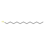
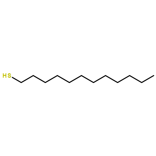
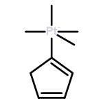
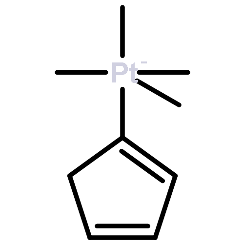
![O-[(2,3,4,5,6-PENTAFLUOROPHENYL)METHYL]HYDROXYLAMINE](http://img.cochemist.com/ccimg/73000/72915-12-9.png)
![O-[(2,3,4,5,6-PENTAFLUOROPHENYL)METHYL]HYDROXYLAMINE](http://img.cochemist.com/ccimg/73000/72915-12-9_b.png)


![[1,1'-Biphenyl]-4-amine,4'-nitro-](http://img.cochemist.com/ccimg/1300/1211-40-1.png)
![[1,1'-Biphenyl]-4-amine,4'-nitro-](http://img.cochemist.com/ccimg/1300/1211-40-1_b.png)


![N-[4-[[(2-amino-3,4-dihydro-4-oxo-6-pteridinyl)methyl]amino]benzoyl]-L-Glutamic acid 5-(2,5-dioxo-1-pyrrolidinyl) ester](http://img.cochemist.com/ccimg/153500/153445-05-7.png)
![N-[4-[[(2-amino-3,4-dihydro-4-oxo-6-pteridinyl)methyl]amino]benzoyl]-L-Glutamic acid 5-(2,5-dioxo-1-pyrrolidinyl) ester](http://img.cochemist.com/ccimg/153500/153445-05-7_b.png)

