Co-reporter:Stuart G. Higgins;Tiziano Agostinelli;Steve Markham;Robert Whiteman
Advanced Materials 2017 Volume 29(Issue 46) pp:
Publication Date(Web):2017/12/01
DOI:10.1002/adma.201703782
AbstractOrganic diodes manufactured on a plastic substrate capable of rectifying a high-frequency radio-frequency identification signal (13.56 MHz), with sufficient power to operate an interactive smart tag, are reported. A high-performance conjugated semiconductor (an indacenodithiophene-benzothiadiazole copolymer) is combined with a carefully optimized architecture to satisfy the electrical requirements for an organic-semiconductor-based logic chip.
Co-reporter:David J. Harkin;Katharina Broch;Maximilian Schreck;Harald Ceymann;Andreas Stoy;Chaw-Keong Yong;Mark Nikolka;Iain McCulloch;Natalie Stingelin;Christoph Lambert
Advanced Materials 2016 Volume 28( Issue 30) pp:6378-6385
Publication Date(Web):
DOI:10.1002/adma.201600851
Co-reporter:Yuanyuan Hu;Vincenzo Pecunia;Lang Jiang;Chong-An Di;Xike Gao
Advanced Materials 2016 Volume 28( Issue 23) pp:4713-4719
Publication Date(Web):
DOI:10.1002/adma.201503812
Co-reporter:Aurélie Y. B. Meneau;Yoann Olivier;Tomas Backlund;Mark James;Dag Werner Breiby;Jens Wenzel Andreasen
Advanced Functional Materials 2016 Volume 26( Issue 14) pp:2326-2333
Publication Date(Web):
DOI:10.1002/adfm.201502502
In solution-processable small molecule semiconductors, the extent of charge carrier wavefunction localization induced by dynamic disorder can be probed spectroscopically as a function of temperature using charge modulation spectroscopy (CMS). Here, it is shown based on combined field-effect transistor and CMS measurements as a function of temperature that in certain molecular semiconductors, such as solution-processible pentacene, charge carriers become trapped at low temperatures in environments in which the charges become highly localized on individual molecules, while in some other molecules the charge carrier wavefunction can retain a degree of delocalization similar to what is present at room temperature. The experimental approach sheds new insight into the nature of shallow charge traps in these materials and allows identifying molecular systems in which intrinsic transport properties could, in principle, be observed at low temperatures if other transport bottlenecks associated with grain boundaries or contacts could be removed.
Co-reporter:Sam Schott;Eliot Gann;Lars Thomsen;Seok-Heon Jung;Jin-Kyun Lee;Christopher R. McNeill
Advanced Materials 2015 Volume 27( Issue 45) pp:7356-7364
Publication Date(Web):
DOI:10.1002/adma.201502437
Co-reporter:Josephine Socratous;Kulbinder K. Banger;Yana Vaynzof;Aditya Sadhanala;Adam D. Brown;Alessro Sepe;Ullrich Steiner
Advanced Functional Materials 2015 Volume 25( Issue 12) pp:1873-1885
Publication Date(Web):
DOI:10.1002/adfm.201404375
The electronic structure of low temperature, solution-processed indium–zinc oxide thin-film transistors is complex and remains insufficiently understood. As commonly observed, high device performance with mobility >1 cm2 V−1 s−1 is achievable after annealing in air above typically 250 °C but performance decreases rapidly when annealing temperatures ≤200 °C are used. Here, the electronic structure of low temperature, solution-processed oxide thin films as a function of annealing temperature and environment using a combination of X-ray photoelectron spectroscopy, ultraviolet photoelectron spectroscopy, and photothermal deflection spectroscopy is investigated. The drop-off in performance at temperatures ≤200 °C to incomplete conversion of metal hydroxide species into the fully coordinated oxide is attributed. The effect of an additional vacuum annealing step, which is beneficial if performed for short times at low temperatures, but leads to catastrophic device failure if performed at too high temperatures or for too long is also investigated. Evidence is found that during vacuum annealing, the workfunction increases and a large concentration of sub-bandgap defect states (re)appears. These results demonstrate that good devices can only be achieved in low temperature, solution-processed oxides if a significant concentration of acceptor states below the conduction band minimum is compensated or passivated by shallow hydrogen and oxygen vacancy-induced donor levels.
Co-reporter:Mathias Gruber, Seok-Heon Jung, Sam Schott, Deepak Venkateshvaran, Auke Jisk Kronemeijer, Jens Wenzel Andreasen, Christopher R. McNeill, Wallace W. H. Wong, Munazza Shahid, Martin Heeney, Jin-Kyun Lee and Henning Sirringhaus
Chemical Science 2015 vol. 6(Issue 12) pp:6949-6960
Publication Date(Web):12 Aug 2015
DOI:10.1039/C5SC01326G
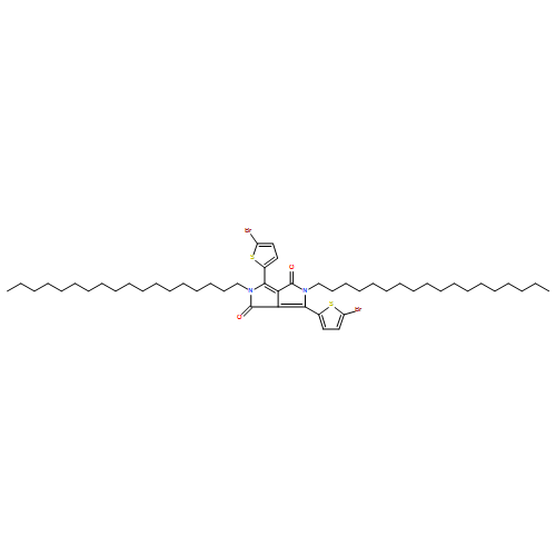
In this article we discuss the synthesis of four new low band-gap co-polymers based on the diketopyrrolopyrrole (DPP) and benzotriazole (BTZ) monomer unit. We demonstrate that the BTZ unit allows for additional solubilizing side-chains on the co-monomer and show that the introduction of a linear side-chain on the DPP-unit leads to an increase in thin-film order and charge-carrier mobility if a sufficiently solubilizing, branched, side chain is attached to the BTZ. We compare two different synthetic routes, direct arylation and Suzuki-polycondensation, by a direct comparison of polymers obtained via the two routes and show that direct arylation produces polymers with lower electrical performance which we attribute to a higher density of chain Furthermore we demonstrate that a polymer utilizing this design motif and synthesized via Suzuki-polycondensation ((l-C18)-DPP-(b-C17)-BTZ) exhibits exceptionally high and near balanced average electron and hole mobilities >2 cm2 V−1 s−1 which are among the highest, robustly extracted mobility values reported for DPP copolymers in a top-gate configuration to date. Our results demonstrate clearly that linear side chain substitution of the DPP unit together with co-monomers that allow for the use of sufficiently long or branched solubilizing side chains can be an attractive design motif for solution processable, high mobility DPP copolymers.
Co-reporter:Milan Vru&x107;ini&x107;;Clemens Matthiesen;Aditya Sadhanala;Giorgio Divitini;Stefania Cacovich;Sian E. Dutton;Caterina Ducati;Mete Atatüre;Henry Snaith;Richard H. Friend;Felix Deschler
Advanced Science 2015 Volume 2( Issue 9) pp:
Publication Date(Web):
DOI:10.1002/advs.201500136
Co-reporter:Vincenzo Pecunia, Kulbinder Banger, Antony Sou, Henning Sirringhaus
Organic Electronics 2015 Volume 21() pp:177-183
Publication Date(Web):June 2015
DOI:10.1016/j.orgel.2015.03.004
•A novel hybrid solution-based complementary integration scheme was developed.•The integration relies on a p-type organic and n-type metal-oxide semiconductor pair.•All integrated transistors share the same solution-processed polymeric dielectric.•The hybrid logic gates give rail-to-rail transitions and ample noise margins.•Logic-gate operation in the megahertz range is achieved via a self-aligned approach.We have developed a novel solution-based integration scheme featuring organic and metal-oxide semiconductors with a polymeric gate dielectric. The integration relies on a facile subtractive patterning technique for the semiconductors, which, through the selection of an appropriate etch stopper, leads to ideal transistor performance. We utilized this novel integration scheme to fabricate self-aligned transistors and logic circuits with a high-mobility p-type conjugated polymer and an n-type amorphous oxide semiconductor, along with a composite polymeric gate dielectric, all solution-deposited by spin coating. The resulting complementary logic gates are capable of rail-to-rail transitions, low-voltage operation down to a 3.5 V power supply, and ample noise margins. Thanks to the self-aligned-gate approach and the state-of-the-art balanced mobilities of the selected semiconductors, our logic gates achieve megahertz operation, thus demonstrating the strength of our hybrid integration scheme.
Co-reporter:Vincenzo Pecunia;Kulbinder Banger
Advanced Electronic Materials 2015 Volume 1( Issue 1-2) pp:
Publication Date(Web):
DOI:10.1002/aelm.201400024
Co-reporter:Auke J. Kronemeijer;Vincenzo Pecunia;Deepak Venkateshvaran;Mark Nikolka;Aditya Sadhanala;John Moriarty;Monika Szumilo
Advanced Materials 2014 Volume 26( Issue 5) pp:728-733
Publication Date(Web):
DOI:10.1002/adma.201303060
Co-reporter:Henning Sirringhaus
Advanced Materials 2014 Volume 26( Issue 9) pp:1319-1335
Publication Date(Web):
DOI:10.1002/adma.201304346
Over the past 25 years, organic field-effect transistors (OFETs) have witnessed impressive improvements in materials performance by 3–4 orders of magnitude, and many of the key materials discoveries have been published in Advanced Materials. This includes some of the most recent demonstrations of organic field-effect transistors with performance that clearly exceeds that of benchmark amorphous silicon-based devices. In this article, state-of-the-art in OFETs are reviewed in light of requirements for demanding future applications, in particular active-matrix addressing for flexible organic light-emitting diode (OLED) displays. An overview is provided over both small molecule and conjugated polymer materials for which field-effect mobilities exceeding > 1 cm2 V–1 s–1 have been reported. Current understanding is also reviewed of their charge transport physics that allows reaching such unexpectedly high mobilities in these weakly van der Waals bonded and structurally comparatively disordered materials with a view towards understanding the potential for further improvement in performance in the future.
Co-reporter:Sungjune Jung;Antony Sou;Kulbinder Banger;Doo-Hyun Ko;Philip C. Y. Chow;Christopher R. McNeill
Advanced Energy Materials 2014 Volume 4( Issue 14) pp:
Publication Date(Web):
DOI:10.1002/aenm.201400432
The prospective of using direct-write printing techniques for the manufacture of organic photovoltaics (OPVs) has made these techniques highly attractive. OPVs have the potential to revolutionize small-scale portable electronic applications by directly providing electric power to the systems. However, no route is available for monolithically integrating the energy-harvesting units into a system in which other components, such as transistors, sensors, or displays, are already fabricated. Here, the fabrication and the measurement of inkjet-printed, air-processed organic solar cells is reported for the first time. Highly controlled conducting and semiconducting films using engineered inks for inkjet printing enable good efficiencies for printed OPVs between ≈2 and 5% power conversion efficiency. The results show that inkjet printing is an attractive digital printing technology for cost-effective, environmentally friendly integration of photovoltaic cells onto plastic substrates.
Co-reporter:Iyad Nasrallah, Kulbinder K. Banger, Yana Vaynzof, Marcia M. Payne, Patrick Too, Jan Jongman, John E. Anthony, and Henning Sirringhaus
Chemistry of Materials 2014 Volume 26(Issue 13) pp:3914
Publication Date(Web):June 11, 2014
DOI:10.1021/cm501397y
We have investigated the degradation effects of ozone exposure on organic field-effect transistors based on 2,8-difluoro-5,11-bis(triethylsilylethynyl)anthradithiophene as the organic semiconducting channel layer, as well as on thin films of this widely used, high-mobility, small molecule semiconductor. Electrical I–V measurements showed a loss of transistor characteristic behavior. We present 1H Nuclear Magnetic Resonance (NMR) spectroscopy results as well as X-ray Photoemission Spectroscopy (XPS) and Fourier Transform Infrared (FTIR) spectroscopy measurements showing the oxidation of the parent molecule, from which we suggest various possible reaction paths.
Co-reporter:Kulbinder K. Banger, Rebecca L. Peterson, Kiyotaka Mori, Yoshihisa Yamashita, Timothy Leedham, and Henning Sirringhaus
Chemistry of Materials 2014 Volume 26(Issue 2) pp:1195
Publication Date(Web):December 22, 2013
DOI:10.1021/cm4035837
Amorphous mixed metal oxides are emerging as high performance semiconductors for thin film transistor (TFT) applications, with indium gallium zinc oxide, InGaZnO (IGZO), being one of the most widely studied and best performing systems. Here, we investigate alkaline earth (barium or strontium) doped InBa(Sr)ZnO as alternative, semiconducting channel layers and compare their performance of the electrical stress stability with IGZO. In films fabricated by solution-processing from metal alkoxide precursors and annealed to 450 °C we achieve high field-effect electron mobility up to 26 cm2 V–1 s–1. We show that it is possible to solution-process these materials at low process temperature (225–200 °C yielding mobilities up to 4.4 cm2 V–1 s–1) and demonstrate a facile “ink-on-demand” process for these materials which utilizes the alcoholysis reaction of alkyl metal precursors to negate the need for complex synthesis and purification protocols. Electrical bias stress measurements which can serve as a figure of merit for performance stability for a TFT device reveal Sr- and Ba-doped semiconductors to exhibit enhanced electrical stability and reduced threshold voltage shift compared to IGZO irrespective of the process temperature and preparation method. This enhancement in stability can be attributed to the higher Gibbs energy of oxidation of barium and strontium compared to gallium.
Co-reporter:Monika M. Szumilo, Eliot H. Gann, Christopher R. McNeill, Vincent Lemaur, Yoann Oliver, Lars Thomsen, Yana Vaynzof, Michael Sommer, and Henning Sirringhaus
Chemistry of Materials 2014 Volume 26(Issue 23) pp:6796
Publication Date(Web):October 23, 2014
DOI:10.1021/cm5033578
Reported here is a characterization of a series of NDI–thiophene copolymers with one, two, three, and four thiophene units synthesized using Stille polycondensation of dibromo-naphthalene diimide and the trimethylstannylthiophene monomers. The effect of extension of the thiophene donor group is studied in terms of structure-charge transport correlation. The influence of side chains located on the thiophene units of copolymers with two and four thiophene units per monomer is also investigated. Charge transport of both signs is studied experimentally in field-effect transistors. Microstructural data obtained by near-edge X-ray absorption fine structure (NEXAFS) and grazing incidence wide-angle X-ray scattering (GIWAXS) is supported by AFM topography scans. Ultraviolet photoelectron spectroscopy (UPS) and UV–vis spectroscopy data are employed in the measurement of energy levels, and changes with annealing temperature are also discussed. Most of the polymers reach excellent electron and hole mobility with one copolymer (NDI-T4) exhibiting an especially balanced ambipolar charge transport of 0.03 cm2 V–1 s–1. An odd–even effect in hole mobility is observed with higher values for polymers with an even number of thiophene units. The reported findings indicate that the final charge transport properties are a result of the interplay of many factors, including crystallinity, planarity and linearity of chain, spacing between acceptor units and packing of solubilizing branched side chains.
Co-reporter:Yuanyuan Hu, Christopher Warwick, Antony Sou, Lang Jiang and Henning Sirringhaus
Journal of Materials Chemistry A 2014 vol. 2(Issue 7) pp:1260-1263
Publication Date(Web):04 Nov 2013
DOI:10.1039/C3TC31869A
We present a new and simple way of fabricating ultra-thin and flexible organic field-effect transistors and circuits by directly peeling them off from conventional SiO2 substrates. The devices show excellent flexibility up to a bending radius of 1 mm. Free-standing OFETs as thin as about 600 nm can also be made in this way. In addition, flexible complementary inverters with a gain of 100 can be fabricated by the peeling-off method.
Co-reporter:T. T. Steckler, M. J. Lee, Z. Chen, O. Fenwick, M. R. Andersson, F. Cacialli and H. Sirringhaus
Journal of Materials Chemistry A 2014 vol. 2(Issue 26) pp:5133-5141
Publication Date(Web):29 May 2014
DOI:10.1039/C4TC00342J
A family of phthalimide–thiophene copolymers with linear and branched alkyl chains attached to the imide nitrogen have been synthesized. Their optical and electronic properties were investigated along with their applications in OFETs and LEFETs. The phthalimide–thiophene copolymer having a C16 straight alkyl chain on the phthalimide yielded the highest mobilities and PLQE with mobilities of 1 × 10⁻³ cm2 V−1 s−1 for holes and 1 × 10⁻² cm2 V−1 s−1 for electrons with a PLQE of ∼28% in the solid state. Since these polymers are ambipolar and emissive, they have proven to be useful for applications as a host material for NIR PLEDs. In this study a 1% loading of NIR emitting DAD segments based on bisthienyl(thiadiazoloquinoxaline) or bisthienyl(benzotriazolothiadiazole) were incorporated into the phthalimide–thiophene polymerization. Using the branched CH(C8H17)2 alkyl chain on the host phthalimide–thiophene copolymer combined with the bisthienyl(benzotriazolothiadiazole) emitter resulted in the most efficient (emission maximum ≥ 850 nm) single layer NIR-emitting PLED to date with an EQE of 0.27% emitting at 885 nm.
Co-reporter:Antony Sou, Sungjune Jung, Enrico Gili, Vincenzo Pecunia, Jerome Joimel, Guillaume Fichet, Henning Sirringhaus
Organic Electronics 2014 Volume 15(Issue 11) pp:3111-3119
Publication Date(Web):November 2014
DOI:10.1016/j.orgel.2014.08.032
•We have fabricated arrays of OTFTs driving an E-Ink display on a flexible transparent plastic foil.•Transistor arrays were configured for different logic functions by inkjet printing silver tracks and PEDOT:PSS resistors.•We demonstrated ring oscillators, flip-flop memories, and a programmable array logic device of 1260 transistors.In this paper, we present a functional integrated plastic system. We have fabricated arrays of organic thin-film transistors (OTFTs) and printed electronic components driving an electrophoretic ink display up to 70 mm by 70 mm on a single flexible transparent plastic foil. Transistor arrays were quickly and reliably configured for different logic functions by an additional process step of inkjet printing conductive silver wires and poly(3,4-ethylenedioxythiophene):poly(styrene sulfonate) (PEDOT:PSS) resistors between transistors or between logic blocks. Among the circuit functions and features demonstrated on the arrays are a 7-stage ring oscillator, a D-type flip-flop memory element, a 2:4 demultiplexer, a programmable array logic device (PAL), and printed wires and resistors. Touch input sensors were also printed, thus only external batteries were required for a complete electronic subsystem. The PAL featured 8 inputs, 8 outputs, 32 product terms, and had 1260 p-type polymer transistors in a 3-metal process using diode-load logic. To the best of our knowledge, this is the first time that a PAL concept with organic transistors has been demonstrated, and also the first time that organic transistors have been used as the control logic for a flexible display which have both been integrated on to a single plastic substrate. The versatility afforded by the additive inkjet printing process is well suited to organic programmable logic on plastic substrates, in effect, making flexible organic electronics more flexible.Figure optionsDownload full-size imageDownload high-quality image (270 K)Download as PowerPoint slide
Co-reporter:Olympia Pachoumi;Cheng Li;Yana Vaynzof;Kulbinder K. Banger
Advanced Energy Materials 2013 Volume 3( Issue 11) pp:1428-1436
Publication Date(Web):
DOI:10.1002/aenm.201300308
Abstract
Stability of organic photovoltaic devices (OPVs) is a limiting factor for their commercialization and still remains a major challenge whilst power conversion efficiencies are now approaching minimum requirements. The inverted organic solar cell (iOSC) architecture shows promising potential for improving significantly the cell's working lifetime. However, when solution processed ZnO is used as electron extraction layer, an undesirable light-soaking step is commonly required before the device reaches a non-permanent maximum performance. This work investigates the use of Sr and Ba doped ZnO films, ZnSrO and ZnBaO, formed by sol-gel deposition using molecular alkoxide precursor solutions, as electron extraction layers in a model iOSCs with poly [3-hexylthiophene] (P3HT): [6, 6]-phenyl C60 butyl acid methyl ester (PCBM) as the active layer. We show that using these ternary oxides the light-soaking step can be circumvented by preventing a dipole forming between the oxide and the active organic layer as supported by electroabsorption spectroscopy measurements of the device built-in field. It is suggested that Sr or Ba doping results in suppression/reduction of the oxygen adsorption at mobile oxygen vacancy sites on the metal oxide surface. Like in thin film transistor (TFT) applications, where materials like InGaZnO are rapidly becoming an important technology, the use of amorphous, mixed metal oxides allows improving the performance and stability of interfacial charge extraction layers for organic solar cells.
Co-reporter:Mi Jung Lee, Zhuoying Chen, Riccardo di Pietro, Martin Heeney, and Henning Sirringhaus
Chemistry of Materials 2013 Volume 25(Issue 10) pp:2075
Publication Date(Web):April 29, 2013
DOI:10.1021/cm400266h
Charge carriers induced in field-effect transistors based on a uniaxially aligned polythiophene polymer, poly(2,5-bis(3-alkylthiophen-2-yl)thieno[3,2-b]thiophene) (PBTTT), are investigated by electrooptical charge modulation spectroscopy (CMS). We used a zone-casting deposition method for uniaxial alignment of the nanoribbon crystalline domains of the polymer and examined the optical anisotropy of neutral and charge induced absorptions in FETs. We find that the charge-induced optical absorptions of the polaronic carriers at the interface exhibit a similar degree of uniaxial anisotropy as the absorption spectrum of the neutral polymer bulk suggesting similar degree of polymer alignment at the interface compared with the bulk. We observe subtle differences in the spectral shape of the polaron absorption polarized along and perpendicular to the polymer chain direction. We also detect an additional charge-induced absorption peak appearing at high charge carrier concentrations, which is similar to the charge-induced absorption that is typical for chemically doped films. These observations provide important insight into the interplay between polaron transport and polymer microstructure.Keywords: aligning polymer; charge induced absorption; organic transistors; polarized spectroscopy;
Co-reporter:Zhuoying Chen;Mi Jung Lee;Raja Shahid Ashraf;Yun Gu;Sebastian Albert-Seifried;Martin Meedom Nielsen;Bob Schroeder;Thomas D. Anthopoulos;Martin Heeney;Iain McCulloch
Advanced Materials 2012 Volume 24( Issue 5) pp:647-652
Publication Date(Web):
DOI:10.1002/adma.201102786
Co-reporter:Michael C. Gwinner;Dinesh Kabra;Matthew Roberts;Thomas J. K. Brenner;Bodo H. Wallikewitz;Christopher R. McNeill;Richard H. Friend
Advanced Materials 2012 Volume 24( Issue 20) pp:2728-2734
Publication Date(Web):
DOI:10.1002/adma.201104602
Co-reporter:Riccardo Di Pietro
Advanced Materials 2012 Volume 24( Issue 25) pp:3367-3372
Publication Date(Web):
DOI:10.1002/adma.201200829
Co-reporter:Riccardo Di Pietro ; Daniele Fazzi ; Tom B. Kehoe
Journal of the American Chemical Society 2012 Volume 134(Issue 36) pp:14877-14889
Publication Date(Web):August 14, 2012
DOI:10.1021/ja304198e
We present an optical spectroscopy study on the role of oxygen and water in electron trapping and storage/bias-stress degradation of n-type polymer field-effect transistors based on one of the most widely studied electron transporting conjugated polymers, poly{[N,N9-bis(2-octyldodecyl)-naphthalene-1,4,5,8-bis(dicarboximide)-2,6-diyl]-alt-5,59-(2,29-bisthiophene)} (P(NDI2OD-T2)). We combine results obtained from charge accumulation spectroscopy, which allow optical quantification of the concentration of mobile and trapped charges in the polymer film, with electrical characterization of P(NDI2OD-T2) organic field-effect transistors to study the mechanism for storage and bias-stress degradation upon exposure to dry air/oxygen and humid nitrogen/water environments, thus separating the effect of the two molecules and determining the nature of their interaction with the polymer. We find that the stability upon oxygen exposure is limited by an interaction between the neutral polymer and molecular oxygen leading to a reduction in electron mobility in the bulk of the semiconductor. We use density functional theory quantum chemical calculations to ascribe the drop in mobility to the formation of a shallow, localized, oxygen-induced trap level, 0.34 eV below the delocalized lowest unoccupied molecular orbital of P(NDI2OD-T2). In contrast, the stability of the polymer anion against water is limited by two competing reactions, one involving the electrochemical oxidation of the polymer anion by water without degradation of the polymer and the other involving a radical anion-catalyzed chemical reaction of the polymer with water, in which the electron can be recycled and lead to further degradation reactions, such that a significant portion of the film is degraded after prolonged bias stressing. Using Raman spectroscopy, we have been able to ascribe this to a chemical interaction of water with the naphthalene diimide unit of the polymer. The degradation mechanisms identified here should be considered to explain electron trapping in other rylene diimides and possibly in other classes of conjugated polymers as well.
Co-reporter:Shrivalli N. Bhat, Riccardo Di Pietro, and Henning Sirringhaus
Chemistry of Materials 2012 Volume 24(Issue 21) pp:4060
Publication Date(Web):October 7, 2012
DOI:10.1021/cm301610w
We report electroluminescence from ion-gel gated, field-effect transistors based on the conjugated polymer, poly(9,9′-dioctylfluorene-co-benzothiadiazole) gated by an 1-ethyl-3-methylimidazoliumbis (trifluoromethylsulfonyl) imide/poly (styrene-block-ethylene oxide-block-styrene) ion gel, and investigate the mechanism for light emission. The devices emit light from near the electron-injecting drain electrode when the drain source voltage exceeds approximately the energy gap of the polymer (Vds> Eg/e). Charge accumulation spectroscopy is used to demonstrate the significant penetration of the negative TFSI– ions into the F8BT assisted by the application of negative gate voltages, where they lead to significant p-type doping of the bulk of the F8BT film. In contrast, no evidence for diffusion of positive ions with positive gate voltages is observed, and this is consistent with the location of the recombination zone in the proximity of electron injecting electrode and the absence of a comparable electron current at positive gate voltages. We conclude that in the light-emission regime the devices operate more akin to a hole-current dominated light-emitting electrochemical cell than a transistor.Keywords: ion gel; light emitting electrochemical cells; light emitting transistors; low voltage operation;
Co-reporter:Michael C. Gwinner, Thomas J. K. Brenner, Jin-Kyun Lee, Carol Newby, Christopher K. Ober, Christopher R. McNeill and Henning Sirringhaus
Journal of Materials Chemistry A 2012 vol. 22(Issue 10) pp:4436-4439
Publication Date(Web):04 Jan 2012
DOI:10.1039/C2JM15715B
Two novel conjugated copolymers based on alkylbenzotriazole and benzothiadiazole with high electron affinities are investigated for applications in polymer field-effect transistors and solar cells. The electron withdrawing nature of these polymers allows for efficient electron injection and transport. We were able to realize ambipolar red light-emitting field-effect transistors with electron mobilities exceeding 0.01 cm2 V−1 s−1 using gold electrodes. All-polymer solar cells with open-circuit voltages larger than 1.2 V using the new polymers as electron acceptor are also demonstrated.
Co-reporter:Dhritiman Gupta, Thomas J.K. Brenner, Sebastian Albert-Seifried, Mi Jung Lee, Martin Heeney, Iain McCulloch, Henning Sirringhaus
Organic Electronics 2012 Volume 13(Issue 1) pp:36-42
Publication Date(Web):January 2012
DOI:10.1016/j.orgel.2011.08.034
A study of photoconductivity in a planar photodiode based on the uniaxially aligned, semicrystalline polymer, poly(2,5-bis(3-alkylthiophene-2-yl)thieno[3,2-b]thiophene) (PBTTT) is presented. The charge carrier photogeneration yield in bulk conjugated polymers is usually low but it could possibly be enhanced by applying a sufficiently large electric field, particularly along the direction of the polymer backbone. PBTTT is, in principle, an ideal system to study any anisotropy in carrier photogeneration because directional alignment of fully extended polymer chains can be achieved over macroscopic length scales. However, we have found that electron trapping in this polymer results in high photoconductive gain obscuring measurements of intrinsic photogeneration. We study the mechanism of photoconductive gain using steady-state and transient photocurrent measurement. Constant background illumination and the deposition of a surface layer of an electron acceptor material have been found to be effective in reducing the gain effects.Graphical abstractHighlights► Photoconductivity anisotropy study with field orientation along the polymer chain and perpendicular to it. ► Highly oriented PBTTT nanoribbon was employed in a lateral geometry photodiode. ► Electron trapping give rise to large photoconductive gain. ► Constant background illumination and deposition of fullerene reduce the photoconductive gain.
Co-reporter:Jennifer R. Moore;Sebastian Albert-Seifried;Akshay Rao;Sylvain Massip;Benjamin Watts;David J. Morgan;Richard H. Friend;Christopher R. McNeill
Advanced Energy Materials 2011 Volume 1( Issue 2) pp:230-240
Publication Date(Web):
DOI:10.1002/aenm.201000035
Abstract
A high electron mobility polymer, poly{[N,N’-bis(2-octyldodecyl)-naphthalene-1,4,5,8-bis(dicarboximide)-2,6-diyl]-alt-5,5’-(2,2’-bithiophene) (P(NDI2OD-T2)) is investigated for use as an electron acceptor in all-polymer blends. Despite the high bulk electron mobility, near-infrared absorption band and compatible energy levels, bulk heterojunction devices fabricated with poly(3-hexylthiophene) (P3HT) as the electron donor exhibit power conversion efficiencies of only 0.2%. In order to understand this disappointing photovoltaic performance, systematic investigations of the photophysics, device physics and morphology of this system are performed. Ultra-fast transient absorption spectroscopy reveals a two-stage decay process with an initial rapid loss of photoinduced polarons, followed by a second slower decay. This second slower decay is similar to what is observed for efficient P3HT:PCBM ([6,6]-phenyl C61-butyric acid methyl ester) blends, however the initial fast decay that is absent in P3HT:PCBM blends suggests rapid, geminate recombination of charge pairs shortly after charge transfer. X-ray microscopy reveals coarse phase separation of P3HT:P(NDI2OD-T2) blends with domains of size 0.2 to 1 micrometer. P3HT photoluminescence, however, is still found to be efficiently quenched indicating intermixing within these mesoscale domains. This hierarchy of phase separation is consistent with the transient absorption, whereby localized confinement of charges on isolated chains in the matrix of the other polymer hinders the separation of interfacial electron-hole pairs. These results indicate that local, interfacial processes are the key factor determining the overall efficiency of this system and highlight the need for improved morphological control in order for the potential benefit of high-mobility electron accepting polymers to be realized.
Co-reporter:Michael C. Gwinner;Riccardo Di Pietro;Yana Vaynzof;Kathryn J. Greenberg;Peter K. H. Ho;Richard H. Friend
Advanced Functional Materials 2011 Volume 21( Issue 8) pp:1432-1441
Publication Date(Web):
DOI:10.1002/adfm.201002696
Abstract
Doping of organic semiconductors (OSCs) with transition metal oxides such as molybdenum trioxide (MoO3) has been used as a powerful method to overcome common issues such as contact resistance and low conductivity, which are limiting factors in organic optoelectronic devices. In this study, the mechanism and efficiency of MoO3-induced p-type doping in OSCs are investigated by means of simultaneous electrical and spectroscopic measurements on lateral diodes. It is demonstrated that energetic changes in the MoO3 energy levels outside vacuum can limit charge-transfer doping and device performance. It is shown and investigated that these changes crucially depend on the OSC. The time evolution of important OSC parameters such as induced charge density, doping concentration and efficiency, conductivity and mobility, is deduced. Moreover, the energetic and chemical changes in MoO3 are investigated via ultraviolet and x-ray photoemission spectroscopy. Combining these experiments, important conclusions are drawn on the time-dependence and stability of MoO3-doping of OSCs, as well as on the processing conditions and device architectures suitable for high-performance devices.
Co-reporter:Mi Jung Lee;Dhritiman Gupta;Ni Zhao;Martin Heeney;Iain McCulloch
Advanced Functional Materials 2011 Volume 21( Issue 5) pp:932-940
Publication Date(Web):
DOI:10.1002/adfm.201001781
Abstract
Charge transport in the ribbon phase of poly(2,5-bis(3-alkylthiophen-2-yl)thieno[3,2-b]thiophene) (PBTTT)—one of the most highly ordered, chain-extended crystalline microstructures available in a conjugated polymer semiconductor—is studied. Ribbon-phase PBTTT has previously been found not to exhibit high carrier mobilities, but it is shown here that field-effect mobilities depend strongly on the device architecture and active interface. When devices are constructed such that the ribbon-phase films are in contact with either a polymer gate dielectric or an SiO2 gate dielectric modified by a hydrophobic, self-assembled monolayer, high mobilities of up to 0.4 cm2 V−1 s−1 can be achieved, which is comparable to those observed previously in terrace-phase PBTTT. In uniaxially aligned, zone-cast films of ribbon-phase PBTTT the mobility anisotropy is measured for transport both parallel and perpendicular to the polymer chain direction. The mobility anisotropy is relatively small, with the mobility along the polymer chain direction being higher by a factor of 3–5, consistent with the grain size encountered in the two transport directions.
Co-reporter:Zhuoying Chen, Junfeng Fang, Feng Gao, Thomas J.K. Brenner, Kulbinder K. Banger, Xingzhu Wang, Wilhelm T.S. Huck, Henning Sirringhaus
Organic Electronics 2011 Volume 12(Issue 3) pp:461-471
Publication Date(Web):March 2011
DOI:10.1016/j.orgel.2010.12.009
We report a comparative study of optical properties, structure and morphology, field-effect transistor (FET) and solar cell performance between poly(4-(3,4′-dihexyl-2,2′-bithiophen-5-yl)-7-(5′-(9,9-dioctyl-9H-fluoren-2-yl)-3,4′-dihexyl-2,2′-bithiophen-5-yl)benzo[c][1,2,5]thiadiazole) (F8TTBTT), and its predecessor poly((9,9-dioctylfluorene)-2,7-diyl-alt-[4,7-bis(3-hexylthien-5-yl)-2,1,3-benzothiadiazole]-2′,2″-diyl) (F8TBT). Compared to F8TBT, F8TTBTT has two more thiophene units incorporated in its monomer structure. Such a modification leads to a reduced optical band gap, improved charge injection and significantly enhanced ambipolar field-effect mobilities reaching 5 × 10⁻² cm2 V−1 s−1 for holes and 4 × 10⁻³ cm2 V−1 s−1 for electrons. The enhanced carrier mobilities are most likely a result of an increased backbone planarization and interchain interaction. As a consequence of ambipolar transport, light-emission was observed from the transistor channel during operation. The reduced band gap and improved charge transport make F8TTBTT an interesting candidate also for solar cell applications. Unoptimized solar cells based on F8TTBTT:PCBM blends were found to exhibit power conversion efficiency under AM 1.5 illumination of ∼1.54%.Graphical abstractOptical micrograph of a F8TTBTT light emitting field-effect transistor under external illumination showing the source–drain electrodes (a) and in operation showing the red light emission from the channel of the device (b).Research highlights► Comparative study of two donor–acceptor polyfluorene copolymers: F8TTBTT and F8TBT. ► F8TTBTT contains more thiophene moieties in its monomer unit compared to F8TBT. ► Enhanced ambipolar charge transport was found in F8TTBTT. ► Correlation between transport and molecular conformation by Raman spectroscopy. ► Realization of light-emitting ambipolar transistors with deep red emission.
Co-reporter:Zhuoying Chen;Henrik Lemke;Sebastian Albert-Seifried;Mario Caironi;Martin Meedom Nielsen;Martin Heeney;Weimin Zhang;Iain McCulloch
Advanced Materials 2010 Volume 22( Issue 21) pp:2371-2375
Publication Date(Web):
DOI:10.1002/adma.200903711
Co-reporter:Henning Sirringhaus;Matt Bird;Ni Zhao
Advanced Materials 2010 Volume 22( Issue 34) pp:3893-3898
Publication Date(Web):
DOI:10.1002/adma.200902857
Abstract
Field-effect transistors based on conjugated polymers are being developed for large-area electronic applications on flexible substrates, but they also provide a very useful tool to probe the charge transport physics of these complex materials. In this review we discuss recent progress in polymer semiconductor materials, which have brought the performance and mobility of polymer devices to levels comparable to that of small-molecule organic semiconductors. These new materials have also enabled deeper insight into the charge transport physics of high-mobility polymer semiconductors gained from experiments with high charge carrier concentration and better molecular-scale understanding of the electronic structure at the semiconductor/dielectric interface.
Co-reporter:Michael C. Gwinner;Yana Vaynzof;Kulbinder K. Banger;Peter K. H. Ho;Richard H. Friend
Advanced Functional Materials 2010 Volume 20( Issue 20) pp:3457-3465
Publication Date(Web):
DOI:10.1002/adfm.201000785
Abstract
Electron injection from the source–drain electrodes limits the performance of many n-type organic field-effect transistors (OFETs), particularly those based on organic semiconductors with electron affinities less than 3.5 eV. Here, it is shown that modification of gold source–drain electrodes with an overlying solution-deposited, patterned layer of an n-type metal oxide such as zinc oxide (ZnO) provides an efficient electron-injecting contact, which avoids the use of unstable low-work-function metals and is compatible with high-resolution patterning techniques such as photolithography. Ambipolar light-emitting field-effect transistors (LEFETs) based on green-light-emitting poly(9,9-dioctylfluorene-alt-benzothiadiazole) (F8BT) and blue-light-emitting poly(9,9-dioctylfluorene) (F8) with electron-injecting gold/ZnO and hole-injecting gold electrodes show significantly lower electron threshold voltages and several orders of magnitude higher ambipolar currents, and hence light emission intensities, than devices with bare gold electrodes. Moreover, different solution-deposited metal oxide injection layers are compared. By spin-coating ZnO from a low-temperature precursor, processing temperatures could be reduced to 150 °C. Ultraviolet photoemission spectroscopy (UPS) shows that the improvement in transistor performance is due to reduction of the electron injection barrier at the interface between the organic semiconductor and ZnO/Au compared to bare gold electrodes.
Co-reporter:Kang-Jun Baeg;Yong-Young Noh;Dong-Yu Kim
Advanced Functional Materials 2010 Volume 20( Issue 2) pp:224-230
Publication Date(Web):
DOI:10.1002/adfm.200901677
Abstract
Organic field-effect transistor (FET) memory is an emerging technology with the potential to realize light-weight, low-cost, flexible charge storage media. Here, solution-processed poly[9,9-dioctylfluorenyl-2,7-diyl]-co-(bithiophene)] (F8T2) nano floating gate memory (NFGM) with a top-gate/bottom-contact device configuration is reported. A reversible shift in the threshold voltage (VTh) and reliable memory characteristics was achieved by the incorporation of thin Au nanoparticles (NPs) as charge storage sites for negative charges (electrons) at the interface between polystyrene and cross-linked poly(4-vinylphenol). The F8T2 NFGM showed relatively high field-effect mobility (µFET) (0.02 cm2 V−1 s−1) for an amorphous semiconducting polymer with a large memory window (ca. 30 V), a high on/off ratio (more than 104) during writing and erasing with an operation voltage of 80 V of gate bias in a relatively short timescale (less than 1 s), and a retention time of a few hours. This top-gated polymer NFGM could be used as an organic transistor memory element for organic flash memory.
Co-reporter:Jui-Fen Chang;Michael C. Gwinner;Mario Caironi;Tomo Sakanoue
Advanced Functional Materials 2010 Volume 20( Issue 17) pp:2825-2832
Publication Date(Web):
DOI:10.1002/adfm.201000436
Abstract
Solution processing of polymer semiconductors provides a new paradigm for large-area electronics manufacturing on flexible substrates, but it also severely restricts the realization of interesting advanced device architectures, such as lateral heterostructures with defined interfaces, which are easily accessible with inorganic materials using photolithography. This is because polymer semiconductors degrade, swell, or dissolve during conventional photoresist processing. Here a versatile, high-resolution photolithographic method is demonstrated for patterning of polymer semiconductors and exemplify this with high-performance p-type and n-type field-effect transistors (FETs) in both bottom- and top-gate architectures, as well as ambipolar light-emitting field-effect transistors (LEFETs), in which the recombination zone can be pinned at a photolithographically defined lateral heterojunction between two semiconducting polymers. The technique therefore enables the realization of a broad range of novel device architectures while retaining optimum materials performance.
Co-reporter:Chuan Liu, Zhihong Liu, Henrik T. Lemke, Hoi Nok Tsao, Ronald C.G. Naber, Yun Li, Kulbinder Banger, Klaus Müllen, Martin M. Nielsen and Henning Sirringhaus
Chemistry of Materials 2010 Volume 22(Issue 6) pp:2120
Publication Date(Web):February 10, 2010
DOI:10.1021/cm902925g
The thin film transistor characteristics of a soluble molecular semiconductor, terrylene tetracarboxdiimide (TDI), a homologue of perylene tetracarboxdiimide (PDI), have been investigated. In a bottom-gate device structure with benzocyclobutene gate dielectric, n-type behavior with electron mobility of 1.1 × 10⁻² cm2 V−1 s−1 has been observed after thermal annealing. When applied in the top-gate structure with a polycyclohexylethylene-based gate dielectric, TDI devices exhibit ambipolar transport with electron and hole mobility of 7.2 × 10⁻³ cm2 V−1 s−1 and 2.2 × 10⁻³ cm2 V−1 s−1 respectively. The correlation between morphology and field-effect mobility was investigated by atomic force microscopy (AFM) and X-ray diffraction (XRD) studies. Spin-coated, annealed TDI film crystallize in a terrace structure, and the molecules are packed in an “edge-on” structure, thus forming a favorable packing arrangement for charge transport in the plane of the film.
Co-reporter:Xiaoyang Cheng, Mario Caironi, Yong-Young Noh, Jianpu Wang, Christopher Newman, He Yan, Antonio Facchetti and Henning Sirringhaus
Chemistry of Materials 2010 Volume 22(Issue 4) pp:1559
Publication Date(Web):January 22, 2010
DOI:10.1021/cm902929b
We demonstrate the use of a cross-linking chemistry for an amorphous fluoropolymer gate dielectric, poly(perfluorobutenylvinylether) commercially known as Cytop. Spin-coated films of Cytop exhibit good gate insulating properties as well as provide excellent OFET operational stability. However, these devices operate at large voltages because the dielectric layer thickness is typically ∼450−600 nm. When the thickness of a Cytop dielectric layer is decreased below 200 nm, the device yields are dramatically reduced due to pinhole formation. Our new cross-linked Cytop (C-Cytop) formulation deposited by spin-coating enables uniform thin films on top of various organic semiconductors that exhibits low gate leakage current densities (<10 nA mm−2) and high dielectric breakdown strengths (>2 MV cm−1). Our approach results in C-Cytop dielectric films as thin as 50 nm, thus allowing the fabrication of reliable p- and n-channel top-gate OFETs operating at very low-voltages (<5 V). The most remarkable properties of this new C-Cytop gate dielectric are the excellent device yields (∼100%) for thicknesses <100 nm and the dramatically reduced sensitivity to the underlying semiconductor film morphology. This new approach represents a significant advance compared to cross-linked PMMA films (C-PMMA) and other nonfluorinated polymer dielectrics on identical test structures. Furthermore, C-Cytop-based OFETs exhibit reduced bias stress and better air stability with respect to C-PMMA because of the inert perfluorinated chemical structure of this polymer. Finally, direct spectroscopic evidence of the cross-linking process was obtained by Fourier transform infrared (FTIR) spectroscopy, demonstrating complete reaction in air and at room temperature.
Co-reporter:Chuan Liu, Henning Sirringhaus
Organic Electronics 2010 Volume 11(Issue 4) pp:558-563
Publication Date(Web):April 2010
DOI:10.1016/j.orgel.2009.12.013
Most conjugated polymer field-effect transistors rely on charge accumulation between an organic semiconductor and a gate dielectric. Much less use has been made of devices based on heterojunctions between two semiconducting polymers. Here we have realized ambipolar polymer field-effect transistors based on bilayers of two polyfluorene-based semiconducting polymers, poly(9,9-dioctylfluorene-alt-N-(4-butylphenyl)diphenylamine) and poly(9,9-dioctylfluorene-alt-benzothiadiazole). We show that the energy offset between the lowest unoccupied molecular orbitals of the two polymers of 1–1.5 eV is sufficient to confine electrons at the bi-layer interface for n-type operation. However, the transfer current–voltage characteristics exhibit an unusual plateau. This is shown to be due to hole charge trapping in donor-like states in the TFB layer during p-type operation.
Co-reporter:Mario Caironi, Enrico Gili, Tomo Sakanoue, Xiaoyang Cheng and Henning Sirringhaus
ACS Nano 2010 Volume 4(Issue 3) pp:1451
Publication Date(Web):February 18, 2010
DOI:10.1021/nn9014664
In this work we demonstrate two building blocks of a scalable manufacturing technology for nanoscale electronic devices based on direct-write printing: an architecture for high-yield printing of electrode gaps with 100 nm dimension and a low-temperature silver complex ink for integration of organic materials with high conductivity metal interconnects. We use single printed droplets that are made to dewet slowly from each other to allow reliable, high yield patterning even in the presence of certain surface defects.Keywords: high resolution printing; inkjet printing; organic field-effect transistor; printed contact array; printed electronics; self-aligned printing; submicrometer channel
Co-reporter:N. Zhao;Y.-Y. Noh;J.-F. Chang;M. Heeney;I. McCulloch;H. Sirringhaus
Advanced Materials 2009 Volume 21( Issue 37) pp:3759-3763
Publication Date(Web):
DOI:10.1002/adma.200900326
Co-reporter:Michael C. Gwinner;Saghar Khodabakhsh;Myoung Hoon Song;Heinz Schweizer;Harald Giessen
Advanced Functional Materials 2009 Volume 19( Issue 9) pp:1360-1370
Publication Date(Web):
DOI:10.1002/adfm.200801897
Abstract
Ambipolar light-emitting organic field-effect transistors (LEFETs) possess the ability to efficiently emit light due to charge recombination in the channel. Since the emission can be made to occur far from the metal electrodes, the LEFET structure has been proposed as a potential architecture for electrically pumped organic lasers. Here, a rib waveguide distributed feedback structure consisting of tantalum pentoxide (Ta2O5) integrated within the channel of a top gate/bottom contact LEFET based on poly(9,9-dioctylfluorene-alt-benzothiadiazole) (F8BT) is demonstrated. The emitted light is coupled efficiently into the resonant mode of the DFB waveguide when the recombination zone of the LEFET is placed directly above the waveguide ridge. This architecture provides strong mode confinement in two dimensions. Mode simulations are used to optimize the dielectric thickness and gate electrode material. It is shown that electrode absorption losses within the device can be eliminated and that the lasing threshold for optical pumping of the LEFET structure with all electrodes (4.5 µJ cm−2) is as low as that of reference devices without electrodes. These results enable quantitative judgement of the prospects for realizing an electrically pumped organic laser based on ambipolar LEFETs. The proposed device provides a powerful, low-loss architecture for integrating high-performance ambipolar organic semiconductor materials into electrically pumped lasing structures.
Co-reporter:Michael C. Gwinner;Saghar Khodabakhsh;Myoung Hoon Song;Heinz Schweizer;Harald Giessen
Advanced Functional Materials 2009 Volume 19( Issue 11) pp:
Publication Date(Web):
DOI:10.1002/adfm.200990048
No abstract is available for this article.
Co-reporter:Xiaoyang Cheng;Yong-Young Noh;Jianpu Wang;Marta Tello;Johannes Frisch;Ralf-Peter Blum;Antje Vollmer;Jürgen P. Rabe;Norbert Koch
Advanced Functional Materials 2009 Volume 19( Issue 15) pp:2407-2415
Publication Date(Web):
DOI:10.1002/adfm.200900315
Abstract
Controlling contact resistance in organic field-effect transistors (OFETs) is one of the major hurdles to achieve transistor scaling and dimensional reduction. In particular in the context of ambipolar and/or light-emitting OFETs it is a difficult challenge to obtain efficient injection of both electrons and holes from one injecting electrode such as gold since organic semiconductors have intrinsically large band gaps resulting in significant injection barrier heights for at least one type of carrier. Here, systematic control of electron and hole contact resistance in poly(9,9-di-n-octylfluorene-alt-benzothiadiazole) ambipolar OFETs using thiol-based self-assembled monolayers (SAMs) is demonstrated. In contrast to common believe, it is found that for a certain SAM the injection of both electrons and holes can be improved. This simultaneous enhancement of electron and hole injection cannot be explained by SAM-induced work-function modifications because the surface dipole induced by the SAM on the metal surface lowers the injection barrier only for one type of carrier, but increases it for the other. These investigations reveal that other key factors also affect contact resistance, including i) interfacial tunneling through the SAM, ii) SAM-induced modifications of interface morphology, and iii) the interface electronic structure. Of particular importance for top-gate OFET geometry is iv) the active polymer layer thickness that dominates the electrode/polymer contact resistance. Therefore, a consistent explanation of how SAM electrode modification is able to improve both electron and hole injection in ambipolar OFETs requires considering all mentioned factors.
Co-reporter:Michael C. Gwinner, Saghar Khodabakhsh, Harald Giessen and Henning Sirringhaus
Chemistry of Materials 2009 Volume 21(Issue 19) pp:4425
Publication Date(Web):September 4, 2009
DOI:10.1021/cm900982a
Ambipolar light-emitting field-effect transistors (LEFETs) based on poly(9,9-dioctylfluorene-alt-benzothiadiazole) (F8BT) are able to combine electrical switching capability with the generation of light within a well-defined recombination zone inside the channel. Therefore, they are an attractive architecture not only for low-loss light signal transmission in optoelectronic integrated circuits but also for the potential realization of electrically pumped organic lasers. However, these applications require a simultaneous optimization of transistor performance and waveguiding of emitted light. Here we show that to achieve efficient waveguiding and optical gain the annealing temperature of the F8BT film has to be kept at 120 °C below its glass transition temperature. At such low processing temperatures it is difficult to achieve efficient ambipolar charge injection from gold source/drain electrodes and charge transport at the active transistor interface. We show that modification of the gold electrodes with a 1-decanethiol self-assembled monolayer (SAM) allows efficient charge injection into F8BT films deposited on top. The performance of such ambipolar LEFETs with SAM-modified electrodes is better than that of devices with bare gold electrodes but processed at higher temperatures.
Co-reporter:Yong-Young Noh, Henning Sirringhaus
Organic Electronics 2009 Volume 10(Issue 1) pp:174-180
Publication Date(Web):February 2009
DOI:10.1016/j.orgel.2008.10.021
We have demonstrated top-gate polymer field-effect transistors (FETs) with ultra-thin (30–50 nm), room-temperature crosslinkable polymer gate dielectrics based on blending an insulating base polymer such as poly(methyl methacrylate) with an organosilane crosslinking agent, 1,6-bis(trichlorosilyl)hexane. The top-gate polymer transistors with thin gate dielectrics were operated at gate voltages less than −8 V with a relatively high dielectric breakdown strength (>3 MV/cm) and a low leakage current (10–100 nA/mm2 at 2 MV/cm). The yield of thin gate dielectrics in top-gate polymer FETs is correlated with the roughness of underlying semiconducting polymer film. High mobilities of 0.1–0.2 cm2/V s and on and off state current ratios of 104 were achieved with the high performance semiconducting polymer, poly(2,5-bis(3-alkylthiophen-2yl)thieno[3,2-b]thiophene.
Co-reporter:J. C. Pinto;G. L. Whiting;S. Khodabakhsh;L. Torre;A. Rodríguez;R. M. Dalgliesh;A. M. Higgins;J. W. Andreasen;M. M. Nielsen;M. Geoghegan;W. T. S. Huck;H. Sirringhaus
Advanced Functional Materials 2008 Volume 18( Issue 1) pp:36-43
Publication Date(Web):
DOI:10.1002/adfm.200700540
Abstract
Low operating voltage is an important requirement that must be met for industrial adoption of organic field-effect transistors (OFETs). We report here solution fabricated polymer brush gate insulators with good uniformity, low surface roughness and high capacitance. These ultra thin polymer films, synthesized by atom transfer radical polymerization (ATRP), were used to fabricate low voltage OFETs with both evaporated pentacene and solution deposited poly(3-hexylthiophene). The semiconductor-dielectric interfaces in these systems were studied with a variety of methods including scanning force microscopy, grazing incidence X-ray diffraction and neutron reflectometry. These studies highlighted key differences between the surfaces of brush and spun cast polymethyl methacrylate (PMMA) films.
Co-reporter:Marta Tello;Marco Chiesa;Claudia M. Duffy
Advanced Functional Materials 2008 Volume 18( Issue 24) pp:3907-3913
Publication Date(Web):
DOI:10.1002/adfm.200800009
Abstract
A scanning Kelvin probe microscopy (SKPM) study of the surface potential of vacuum sublimed pentacene transistors under bias stress and its correlation with the film morphology is presented. While for thicker films there are some trapping centers inhomogeneously distributed over the film, as previously reported by other authors, by decreasing the film thickness the effect of thin intergrain regions (IGRs) becomes clear and a very good correlation between the topography and the potential data is observed. It is shown that in the thick pentacene grains the potential is homogeneous and independent of the gate bias applied with negligible charge trapping, while in the thin IGRs the potential varies with the applied gate bias, indicating that only an incomplete accumulation layer can be formed. Clear evidence for preferential charge trapping in the thin IGRs is obtained.
Co-reporter:Jana Zaumseil;Chris Groves;Jessica M. Winfield;Neil C. Greenham
Advanced Functional Materials 2008 Volume 18( Issue 22) pp:3630-3637
Publication Date(Web):
DOI:10.1002/adfm.200800863
Abstract
A promising, general strategy for improving performance of optoelectronic devices based on conjugated polymer semiconductors is to make better use of the fast intrachain transport along the covalently bonded polymer backbone. Little is known, however, about how the recombination rate between electrons and holes would be affected in device structures in which current flow is primarily along the polymer chain. Here a light-emitting field effect transistor (LFET) structure with a uniaxially aligned semiconducting polymer is used to show that the width and shape of the recombination zone depend strongly on polymer alignment. For alignment of the polymer parallel to the current the emission zone is 5–10 times wider than for perpendicular alignment. 2D drift-diffusion modeling is used to show that such significant widening of the recombination zone in the case of parallel alignment implies that the recombination rate constant is more than 100 times lower than expected for standard Langevin recombination. On the basis of Monte Carlo modeling it is proposed that such unexpected weak recombination is a result of the significant mobility anisotropy of the aligned polymer. These results provide new fundamental insight into the recombination physics of polymer semiconductors.
Co-reporter:Claudia M. Duffy, Jens W. Andreasen, Dag W. Breiby, Martin M. Nielsen, Masahiko Ando, Takashi Minakata and Henning Sirringhaus
Chemistry of Materials 2008 Volume 20(Issue 23) pp:7252
Publication Date(Web):November 6, 2008
DOI:10.1021/cm801689f
We investigate the growth and field-effect transistor performance of aligned pentacene thin films deposited by zone-casting from a solution of unsubstituted pentacene molecules in a chlorinated solvent. Polarized optical microscopy shows that solution processed pentacene films grow as large crystalline domains with pronounced anisotropy in the substrate plane, in contrast to vacuum sublimed pentacene films, which consist of small crystalline grains with random in-plane orientation. The high structural alignment is confirmed by in-plane and out-of-plane X-ray diffraction analysis, with out-of-plane 00n reflections up to at least the seventh order, and a pronounced in-plane anisotropy with the a-axis of the triclinic unit cell predominantly aligned parallel to the zone-casting direction and the ab-plane parallel to the substrate. The average charge carrier mobility of the zone-cast pentacene devices depends strongly on the underlying dielectric. Divinylsiloxane-bis-benzocyclobutene (BCB) resin is found to be a suitable gate dielectric allowing reproducible film deposition and high field-effect mobilities up to 0.4−0.7 cm2/(V s) and on/off ratios of 106−107. A small mobility anisotropy is observed for devices with channels aligned along and perpendicular to the zone-casting direction.
Co-reporter:J. Zaumseil;J.-S. Kim;R. H. Friend;C. L. Donley;H. Sirringhaus
Advanced Materials 2006 Volume 18(Issue 20) pp:
Publication Date(Web):10 OCT 2006
DOI:10.1002/adma.200690083
The inside cover shows light emission from within the channel of an ambipolar field-effect transistor based on the green-light-emitting conjugated polymer F8BT in a bottom contact/top gate structure, as reported by Sirringhaus and co-workers on p. 2708. It visually demonstrates the formation of separate electron and hole accumulation layers in ambipolar transistors and radiative recombination of charge carriers where the two layers meet (schematic), which is controlled by the applied voltages.
Co-reporter:J.-S. Kim;C. L. Donley;H. Sirringhaus;J. Zaumseil;R. H. Friend
Advanced Materials 2006 Volume 18(Issue 20) pp:2708-2712
Publication Date(Web):20 SEP 2006
DOI:10.1002/adma.200601080
Bright, ambipolar, light-emitting polymer field-effect transistors in a bottom-contact/top-gate structure using poly(9,9-di-n-octylfluorene-alt- benzothiadiazole) (F8BT) as a green-emitting semiconductor show balanced hole and electron mobilities, depending on the polymer dielectric. The emission zone, observed as a bright line in the figure, is well defined and can be moved through the channel.
Co-reporter:Mathias Gruber, Seok-Heon Jung, Sam Schott, Deepak Venkateshvaran, Auke Jisk Kronemeijer, Jens Wenzel Andreasen, Christopher R. McNeill, Wallace W. H. Wong, Munazza Shahid, Martin Heeney, Jin-Kyun Lee and Henning Sirringhaus
Chemical Science (2010-Present) 2015 - vol. 6(Issue 12) pp:NaN6960-6960
Publication Date(Web):2015/08/12
DOI:10.1039/C5SC01326G
In this article we discuss the synthesis of four new low band-gap co-polymers based on the diketopyrrolopyrrole (DPP) and benzotriazole (BTZ) monomer unit. We demonstrate that the BTZ unit allows for additional solubilizing side-chains on the co-monomer and show that the introduction of a linear side-chain on the DPP-unit leads to an increase in thin-film order and charge-carrier mobility if a sufficiently solubilizing, branched, side chain is attached to the BTZ. We compare two different synthetic routes, direct arylation and Suzuki-polycondensation, by a direct comparison of polymers obtained via the two routes and show that direct arylation produces polymers with lower electrical performance which we attribute to a higher density of chain Furthermore we demonstrate that a polymer utilizing this design motif and synthesized via Suzuki-polycondensation ((l-C18)-DPP-(b-C17)-BTZ) exhibits exceptionally high and near balanced average electron and hole mobilities >2 cm2 V−1 s−1 which are among the highest, robustly extracted mobility values reported for DPP copolymers in a top-gate configuration to date. Our results demonstrate clearly that linear side chain substitution of the DPP unit together with co-monomers that allow for the use of sufficiently long or branched solubilizing side chains can be an attractive design motif for solution processable, high mobility DPP copolymers.
Co-reporter:Yuanyuan Hu, Christopher Warwick, Antony Sou, Lang Jiang and Henning Sirringhaus
Journal of Materials Chemistry A 2014 - vol. 2(Issue 7) pp:NaN1263-1263
Publication Date(Web):2013/11/04
DOI:10.1039/C3TC31869A
We present a new and simple way of fabricating ultra-thin and flexible organic field-effect transistors and circuits by directly peeling them off from conventional SiO2 substrates. The devices show excellent flexibility up to a bending radius of 1 mm. Free-standing OFETs as thin as about 600 nm can also be made in this way. In addition, flexible complementary inverters with a gain of 100 can be fabricated by the peeling-off method.
Co-reporter:T. T. Steckler, M. J. Lee, Z. Chen, O. Fenwick, M. R. Andersson, F. Cacialli and H. Sirringhaus
Journal of Materials Chemistry A 2014 - vol. 2(Issue 26) pp:NaN5141-5141
Publication Date(Web):2014/05/29
DOI:10.1039/C4TC00342J
A family of phthalimide–thiophene copolymers with linear and branched alkyl chains attached to the imide nitrogen have been synthesized. Their optical and electronic properties were investigated along with their applications in OFETs and LEFETs. The phthalimide–thiophene copolymer having a C16 straight alkyl chain on the phthalimide yielded the highest mobilities and PLQE with mobilities of 1 × 10⁻³ cm2 V−1 s−1 for holes and 1 × 10⁻² cm2 V−1 s−1 for electrons with a PLQE of ∼28% in the solid state. Since these polymers are ambipolar and emissive, they have proven to be useful for applications as a host material for NIR PLEDs. In this study a 1% loading of NIR emitting DAD segments based on bisthienyl(thiadiazoloquinoxaline) or bisthienyl(benzotriazolothiadiazole) were incorporated into the phthalimide–thiophene polymerization. Using the branched CH(C8H17)2 alkyl chain on the host phthalimide–thiophene copolymer combined with the bisthienyl(benzotriazolothiadiazole) emitter resulted in the most efficient (emission maximum ≥ 850 nm) single layer NIR-emitting PLED to date with an EQE of 0.27% emitting at 885 nm.
Co-reporter:Michael C. Gwinner, Thomas J. K. Brenner, Jin-Kyun Lee, Carol Newby, Christopher K. Ober, Christopher R. McNeill and Henning Sirringhaus
Journal of Materials Chemistry A 2012 - vol. 22(Issue 10) pp:NaN4439-4439
Publication Date(Web):2012/01/04
DOI:10.1039/C2JM15715B
Two novel conjugated copolymers based on alkylbenzotriazole and benzothiadiazole with high electron affinities are investigated for applications in polymer field-effect transistors and solar cells. The electron withdrawing nature of these polymers allows for efficient electron injection and transport. We were able to realize ambipolar red light-emitting field-effect transistors with electron mobilities exceeding 0.01 cm2 V−1 s−1 using gold electrodes. All-polymer solar cells with open-circuit voltages larger than 1.2 V using the new polymers as electron acceptor are also demonstrated.

![Pyrrolo[3,4-c]pyrrole-1,4-dione, 2,5-dihydro-2,5-bis(2-octyldodecyl)-3,6-di-2-thienyl-](/data/chemimg/139000/1267540-02-2.png)
![Pyrrolo[3,4-c]pyrrole-1,4-dione, 2,5-dihydro-2,5-bis(2-octyldodecyl)-3,6-di-2-thienyl-](/data/chemimg/139000/1267540-02-2_b.png)


![Pentacene, 1,4,8,11-tetramethyl-6,13-bis[2-(triethylsilyl)ethynyl]-](/data/chemimg/3755000/1173698-76-4.png)
![Pentacene, 1,4,8,11-tetramethyl-6,13-bis[2-(triethylsilyl)ethynyl]-](/data/chemimg/3755000/1173698-76-4_b.png)


![4,7-Dibromo-2-octyl-2H-benzo[d][1,2,3]triazole](http://img.cochemist.com/ccimg/960600/960509-83-5.png)
![4,7-Dibromo-2-octyl-2H-benzo[d][1,2,3]triazole](http://img.cochemist.com/ccimg/960600/960509-83-5_b.png)
![[1]benzothieno[3,2-b][1]benzothiophene, 2,7-dioctyl-](http://img.cochemist.com/ccimg/583100/583050-70-8.png)
![[1]benzothieno[3,2-b][1]benzothiophene, 2,7-dioctyl-](http://img.cochemist.com/ccimg/583100/583050-70-8_b.png)
![Poly[(9,9-dioctylfluorenyl-2,7-diyl)-alt-(benzo[2,1,3]thiadiazol-4,7-diyl)]](/data/chemimg/107700/210347-52-7.png)
![Poly[(9,9-dioctylfluorenyl-2,7-diyl)-alt-(benzo[2,1,3]thiadiazol-4,7-diyl)]](/data/chemimg/107700/210347-52-7_b.png)


![Anthra[2,3-b:6,7-b']dithiophene, 2,8-difluoro-5,11-bis[2-(triethylsilyl)ethynyl]-](/data/chemimg/324700/1015071-21-2.png)
![Anthra[2,3-b:6,7-b']dithiophene, 2,8-difluoro-5,11-bis[2-(triethylsilyl)ethynyl]-](/data/chemimg/324700/1015071-21-2_b.png)


![Poly[2,5-bis(3-tetradecylthiophen-2-yl)thieno[3,2-b]thiophene]](http://img.cochemist.com/ccimg/888500/888491-19-8.png)
![Poly[2,5-bis(3-tetradecylthiophen-2-yl)thieno[3,2-b]thiophene]](http://img.cochemist.com/ccimg/888500/888491-19-8_b.png)