Co-reporter:Hanna M. Nilsson, Brendan Meany, Jeremy Ticey, Chuan-Fu Sun, YuHuang Wang, and John Cumings
Langmuir 2015 Volume 31(Issue 25) pp:6948-6955
Publication Date(Web):May 28, 2015
DOI:10.1021/acs.langmuir.5b01175
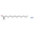
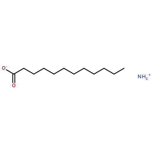
Experiments probing the properties of individual carbon nanotubes (CNTs) and those measuring bulk composites show vastly different results. One major issue limiting the results is that the procedures required to separate and test CNTs introduce contamination that changes the properties of the CNT. These contamination residues often come from the resist used in lithographic processing and the surfactant used to suspend and deposit the CNTs, commonly sodium dodecyl sulfate (SDS). Here we present ammonium laurate (AL), a surfactant that has previously not been used for this application, which differs from SDS only by substitution of ionic constituents but shows vastly cleaner depositions. In addition, we show that compared to SDS, AL-suspended CNTs have greater shelf stability and more selective dispersion. These results are verified using transmission electron microscopy, atomic force microscopy, ζ-potential measurements, and Raman and absorption optical spectroscopy. This surfactant is simple to prepare, and the nanotube solutions require minimal sonication and centrifugation in order to outperform SDS.
Co-reporter:Kai He and John Cumings
Nano Letters 2013 Volume 13(Issue 10) pp:4815-4819
Publication Date(Web):August 26, 2013
DOI:10.1021/nl402509c
We present the direct observation, using off-axis electron holography (EH), of the electric potential distribution in the vicinity of a single carbon nanotube electrically biased by two closely spaced contacts. When our results are combined with finite element modeling, we demonstrate the ability to separately observe the electrostatic potential drops across the metal contacts at the interface with the nanotube and along the length of the nanotube itself. We demonstrate that the uneven resistivity of different contacts can cause an asymmetric EH phase shift, which can readily be identified and quantified. EH thus offers a unique and precise approach for in-depth understanding and quick diagnosis of many similar nanoscale electronic devices.
Co-reporter:Khim Karki, Yujie Zhu, Yihang Liu, Chuan-Fu Sun, Liangbing Hu, YuHuang Wang, Chunsheng Wang, and John Cumings
ACS Nano 2013 Volume 7(Issue 9) pp:8295
Publication Date(Web):August 29, 2013
DOI:10.1021/nn403895h
The engineering of hollow nanostructures is a promising approach to addressing instabilities in silicon-based electrodes for lithium-ion batteries. Previous studies showed that a SiOx coating on silicon nanotubes (SiNTs) could function as a constraining layer and enhance capacity retention in electrodes with low mass loading, but we show here that similarly produced electrodes having negligible SiOx coating and significantly higher mass loading show relatively low capacity retention, fading quickly within the early cycles. We find that the SiNT performance can still be enhanced, even in electrodes with high mass loading, by the use of Ni functional coatings on the outer surface, leading to greatly enhanced capacity retention in a manner that could scale better to industrially relevant battery capacities. In situ transmission electron microscopy studies reveal that the Ni coatings suppress the Si wall from expanding outward, instead carrying the large hoop stress and forcing the Si to expand inward toward the hollow inner core. Evidence shows that these controlled volume changes in Ni-coated SiNTs, accompanied by the electrochemically inert nature of Ni coatings, unlike SiOx, may enhance the stability of the electrolyte at the outer surface against forming a thick solid electrolyte interphase (SEI) layer. These results provide useful guidelines for designing nanostructured silicon electrodes for viable lithium-ion battery applications.Keywords: in situ TEM; nickel coating; SEI; silicon nanotubes; stability
Co-reporter:Chuan-Fu Sun, Khim Karki, Zheng Jia, Hongwei Liao, Yin Zhang, Teng Li, Yue Qi, John Cumings, Gary W. Rubloff, and YuHuang Wang
ACS Nano 2013 Volume 7(Issue 3) pp:2717
Publication Date(Web):February 12, 2013
DOI:10.1021/nn4001512
Interfacial instability is a fundamental issue in heterostructures ranging from biomaterials to joint replacement and electronic packaging. This challenge is particularly intriguing for lithium ion battery anodes comprising silicon as the ion storage material, where ultrahigh capacity is accompanied by vast mechanical stress that threatens delamination of silicon from the current collectors at the other side of the interface. Here, we describe Si-beaded carbon nanotube (CNT) strings whose interface is controlled by chemical functionalization, producing separated amorphous Si beads threaded along mechanically robust and electrically conductive CNT. In situ transmission electron microscopy combined with atomic and continuum modeling reveal that the chemically tailored Si–C interface plays important roles in constraining the Si beads, such that they exhibit a symmetric “radial breathing” around the CNT string, remaining crack-free and electrically connected throughout lithiation–delithiation cycling. These findings provide fundamental insights in controlling nanostructured interfaces to effectively respond to demanding environments such as lithium batteries.Keywords: carbon nanotube; in situ TEM; interface; lithium ion battery; modeling; nanofabrication; propagation
Co-reporter:Khim Karki, Eric Epstein, Jeong-Hyun Cho, Zheng Jia, Teng Li, S. Tom Picraux, Chunsheng Wang, and John Cumings
Nano Letters 2012 Volume 12(Issue 3) pp:1392-1397
Publication Date(Web):February 16, 2012
DOI:10.1021/nl204063u
From in situ transmission electron microscopy (TEM) observations, we present direct evidence of lithium-assisted welding between physically contacted silicon nanowires (SiNWs) induced by electrochemical lithiation and delithiation. This electrochemical weld between two SiNWs demonstrates facile transport of lithium ions and electrons across the interface. From our in situ observations, we estimate the shear strength of the welded region after delithiation to be approximately 200 MPa, indicating that a strong bond is formed at the junction of two SiNWs. This welding phenomenon could help address the issue of capacity fade in nanostructured silicon battery electrodes, which is typically caused by fracture and detachment of active materials from the current collector. The process could provide for more robust battery performance either through self-healing of fractured components that remain in contact or through the formation of a multiconnected network architecture.
Co-reporter:Hongwei Liao;Khim Karki;Yin Zhang;YuHuang Wang
Advanced Materials 2011 Volume 23( Issue 37) pp:4318-4322
Publication Date(Web):
DOI:10.1002/adma.201101762
Co-reporter:Jia Huang, Daniel R. Hines, Byung Jun Jung, Merijntje S. Bronsgeest, Andrew Tunnell, Vince Ballarotto, Howard E. Katz, Michael S. Fuhrer, Ellen D. Williams, John Cumings
Organic Electronics 2011 Volume 12(Issue 9) pp:1471-1476
Publication Date(Web):September 2011
DOI:10.1016/j.orgel.2011.05.021
Solution processed organic field-effect transistors (OFETs) usually have high on/off ratios but suffer from low mobilities, while transistors based on graphene usually exhibit very high mobilities but low on/off ratios. We demonstrate a straightforward route to solve the challenging problem of enhancing the effective mobility in OFETs while keeping the on/off ratio sufficiently high. We achieve this by developing hybrid FETs incorporating both organic semiconductors and graphene. Compared against OFETs with only pure organic semiconductors, our hybrid FETs exhibit up to 20 times higher effective mobilities, and yet they keep the on/off ratios comparable or better. P3HT/graphene hybrid FETs exhibit mobility as high as 0.17 cm2 V−1 s−1, and PQT-12/graphene hybrid FETs show effective mobility up to 0.6 cm2 V−1 s−1. We expect that incorporating graphene is a general route to enhance the performance of OFETs, providing a low-cost avenue for enhancing OFET performance.Graphical abstractOrganic semiconductor/graphene hybrid field-effect transistors (FETs) are fabricated by solution processes. Compared to FETs with pure organic semiconductors, hybrid FETs exhibit 20 times higher effective mobility while keeping the on/off ratio of devices sufficiently high.Highlights► We report a straightforward route to enhance the mobility in OFETs. ► Hybrid FETs incorporating both organic semiconductors and graphene were developed. ► Hybrid FETs exhibit up to 20 times higher effective mobilities than pure OFETs without graphene. ► P3HT/graphene hybrid FETs exhibit mobility as high as 0.17 cm2 V−1 s−1. ► PQT-12/graphene hybrid FETs show effective mobility up to 0.6 cm2 V−1 s−1.
Co-reporter:Todd Brintlinger, Sung-Hwan Lim, Kamal H. Baloch, Paris Alexander, Yi Qi, John Barry, John Melngailis, Lourdes Salamanca-Riba, I. Takeuchi and John Cumings
Nano Letters 2010 Volume 10(Issue 4) pp:1219-1223
Publication Date(Web):March 3, 2010
DOI:10.1021/nl9036406
We report direct observation of controlled and reversible switching of magnetic domains using static (dc) electric fields applied in situ during Lorentz microscopy. The switching is realized through electromechanical coupling in thin film Fe0.7Ga0.3/BaTiO3 bilayer structures mechanically released from the growth substrate. The domain wall motion is observed dynamically, allowing the direct association of local magnetic ordering throughout a range of applied electric fields. During application of ∼7−11 MV/m electric fields to the piezoelectric BaTiO3 film, local magnetic domains rearrange in the ferromagnetic Fe0.7Ga0.3 layer due to the transfer of strain from the BaTiO3 film. A simulation based on micromagnetic modeling shows a magnetostrictive anisotropy of 25 kPa induced in the Fe0.7Ga0.3 due to the strain. This electric-field-dependent uniaxial anisotropy is proposed as a possible mechanism to control the coercive field during operation of an integrated magnetoelectric memory node.