Co-reporter:Matthew D. Smith, Brian L. Watson, Reinhold H. Dauskardt, and Hemamala I. Karunadasa
Chemistry of Materials September 12, 2017 Volume 29(Issue 17) pp:7083-7083
Publication Date(Web):August 17, 2017
DOI:10.1021/acs.chemmater.7b02594
Co-reporter:Adam Jaffe, Yu Lin, Wendy L. Mao, and Hemamala I. Karunadasa
Journal of the American Chemical Society March 29, 2017 Volume 139(Issue 12) pp:4330-4330
Publication Date(Web):March 14, 2017
DOI:10.1021/jacs.7b01162
We report the metallization of the hybrid perovskite semiconductor (MA)PbI3 (MA = CH3NH3+) with no apparent structural transition. We tracked its bandgap evolution during compression in diamond-anvil cells using absorption spectroscopy and observed strong absorption over both visible and IR wavelengths at pressures above ca. 56 GPa, suggesting the imminent closure of its optical bandgap. The metallic character of (MA)PbI3 above 60 GPa was confirmed using both IR reflectivity and variable-temperature dc conductivity measurements. The impressive semiconductor properties of halide perovskites have recently been exploited in a multitude of optoelectronic applications. Meanwhile, the study of metallic properties in oxide perovskites has revealed diverse electronic phenomena. Importantly, the mild synthetic routes to halide perovskites and the templating effects of the organic cations allow for fine structural control of the inorganic lattice. Pressure-induced closure of the 1.6 eV bandgap in (MA)PbI3 demonstrates the promise of the continued study of halide perovskites under a range of thermodynamic conditions, toward realizing wholly new electronic properties.
Co-reporter:Adam Jaffe, Yu Lin, and Hemamala I. Karunadasa
ACS Energy Letters July 14, 2017 Volume 2(Issue 7) pp:1549-1549
Publication Date(Web):May 31, 2017
DOI:10.1021/acsenergylett.7b00284
Lattice compression allows for systematic structural tuning without changing composition. Halide perovskites are a large and diverse family of solids, which have enormous potential for applications in energy capture, storage, and utilization. Notably, they have soft lattices and their photophysical and transport properties exhibit a large pressure response. In this Perspective, we highlight how pressure can alter their electronic landscapes, affect excited-state dynamics, and afford new structures not accessible through conventional syntheses. We further discuss how the insight we gain from high-pressure studies expands the scope of these versatile materials in current and future energy applications.
Co-reporter:Adam H. Slavney, Linn Leppert, Davide Bartesaghi, Aryeh Gold-Parker, Michael F. Toney, Tom J. Savenije, Jeffrey B. Neaton, and Hemamala I. Karunadasa
Journal of the American Chemical Society April 12, 2017 Volume 139(Issue 14) pp:5015-5015
Publication Date(Web):March 29, 2017
DOI:10.1021/jacs.7b01629
Halide double perovskites have recently been developed as less toxic analogs of the lead perovskite solar-cell absorbers APbX3 (A = monovalent cation; X = Br or I). However, all known halide double perovskites have large bandgaps that afford weak visible-light absorption. The first halide double perovskite evaluated as an absorber, Cs2AgBiBr6 (1), has a bandgap of 1.95 eV. Here, we show that dilute alloying decreases 1’s bandgap by ca. 0.5 eV. Importantly, time-resolved photoconductivity measurements reveal long-lived carriers with microsecond lifetimes in the alloyed material, which is very promising for photovoltaic applications. The alloyed perovskite described herein is the first double perovskite to show comparable bandgap energy and carrier lifetime to those of (CH3NH3)PbI3. By describing how energy- and symmetry-matched impurity orbitals, at low concentrations, dramatically alter 1’s band edges, we open a potential pathway for the large and diverse family of halide double perovskites to compete with APbX3 absorbers.
Co-reporter:Adam H. Slavney, Rebecca W. Smaha, Ian C. Smith, Adam Jaffe, Daiki Umeyama, and Hemamala I. Karunadasa
Inorganic Chemistry 2017 Volume 56(Issue 1) pp:46-55
Publication Date(Web):August 5, 2016
DOI:10.1021/acs.inorgchem.6b01336
The impressive rise in efficiencies of solar cells employing the three-dimensional (3D) lead–iodide perovskite absorbers APbI3 (A = monovalent cation) has generated intense excitement. Although these perovskites have remarkable properties as solar-cell absorbers, their potential commercialization now requires a greater focus on the materials’ inherent shortcomings and environmental impact. This creates a challenge and an opportunity for synthetic chemists to address these issues through the design of new materials. Synthetic chemistry offers powerful tools for manipulating the magnificent flexibility of the perovskite lattice to expand the number of functional analogues to APbI3. To highlight improvements that should be targeted in new materials, here we discuss the intrinsic instability and toxicity of 3D lead–halide perovskites. We consider possible sources of these instabilities and propose methods to overcome them through synthetic design. We also discuss new materials developed for realizing the exceptional photophysical properties of lead–halide perovskites in more environmentally benign materials. In this Forum Article, we provide a brief overview of the field with a focus on our group’s contributions to identifying and addressing problems inherent to 3D lead–halide perovskites.
Co-reporter:Matthew D. Smith;Adam Jaffe;Emma R. Dohner;Aaron M. Lindenberg
Chemical Science (2010-Present) 2017 vol. 8(Issue 6) pp:4497-4504
Publication Date(Web):2017/05/30
DOI:10.1039/C7SC01590A
Through structural and optical studies of a series of two-dimensional hybrid perovskites, we show that broadband emission upon near-ultraviolet excitation is common to (001) lead-bromide perovskites. Importantly, we find that the relative intensity of the broad emission correlates with increasing out-of-plane distortion of the Pb–(μ-Br)–Pb angle in the inorganic sheets. Temperature- and power-dependent photoluminescence data obtained on a representative (001) perovskite support an intrinsic origin to the broad emission from the bulk material, where photogenerated carriers cause excited-state lattice distortions mediated through electron–lattice coupling. In contrast, most inorganic phosphors contain extrinsic emissive dopants or emissive surface sites. The design rules established here could allow us to systematically optimize white-light emission from layered hybrid perovskites by fine-tuning the bulk crystal structure.
Co-reporter:Matthew D. Smith;Laurent Pedesseau;Mikaël Kepenekian;Ian C. Smith;Claudine Katan;Jacky Even
Chemical Science (2010-Present) 2017 vol. 8(Issue 3) pp:1960-1968
Publication Date(Web):2017/02/28
DOI:10.1039/C6SC02848A
We show that post-synthetic small-molecule intercalation can significantly reduce the electronic confinement of 2D hybrid perovskites. Using a combined experimental and theoretical approach, we explain structural, optical, and electronic effects of intercalating highly polarizable molecules in layered perovskites designed to stabilize the intercalants. Polarizable molecules in the organic layers substantially alter the optical and electronic properties of the inorganic layers. By calculating the spatially resolved dielectric profiles of the organic and inorganic layers within the hybrid structure, we show that the intercalants afford organic layers that are more polarizable than the inorganic layers. This strategy reduces the confinement of excitons generated in the inorganic layers and affords the lowest exciton binding energy for an n = 1 perovskite of which we are aware. We also demonstrate a method for computationally evaluating the exciton's binding energy by solving the Bethe–Salpeter equation for the exciton, which includes an ab initio determination of the material's dielectric profile across organic and inorganic layers. This new semi-empirical method goes beyond the imprecise phenomenological approximation of abrupt dielectric-constant changes at the organic–inorganic interfaces. This work shows that incorporation of polarizable molecules in the organic layers, through intercalation or covalent attachment, is a viable strategy for tuning 2D perovskites towards mimicking the reduced electronic confinement and isotropic light absorption of 3D perovskites while maintaining the greater synthetic tunability of the layered architecture.
Co-reporter:Adam H. Slavney; Te Hu; Aaron M. Lindenberg
Journal of the American Chemical Society 2016 Volume 138(Issue 7) pp:2138-2141
Publication Date(Web):February 7, 2016
DOI:10.1021/jacs.5b13294
Despite the remarkable rise in efficiencies of solar cells containing the lead-halide perovskite absorbers RPbX3 (R = organic cation; X = Br– or I–), the toxicity of lead remains a concern for the large-scale implementation of this technology. This has spurred the search for lead-free materials with similar optoelectronic properties. Here, we use the double-perovskite structure to incorporate nontoxic Bi3+ into the perovskite lattice in Cs2AgBiBr6 (1). The solid shows a long room-temperature fundamental photoluminescence (PL) lifetime of ca. 660 ns, which is very encouraging for photovoltaic applications. Comparison between single-crystal and powder PL decay curves of 1 suggests inherently high defect tolerance. The material has an indirect bandgap of 1.95 eV, suited for a tandem solar cell. Furthermore, 1 is significantly more heat and moisture stable compared to (MA)PbI3. The extremely promising optical and physical properties of 1 shown here motivate further exploration of both inorganic and hybrid halide double perovskites for photovoltaics and other optoelectronics.
Co-reporter:Daiki Umeyama, Yu Lin, and Hemamala I. Karunadasa
Chemistry of Materials 2016 Volume 28(Issue 10) pp:3241
Publication Date(Web):May 9, 2016
DOI:10.1021/acs.chemmater.6b01147
Co-reporter:Adam Jaffe, Yu Lin, Christine M. Beavers, Johannes Voss, Wendy L. Mao, and Hemamala I. Karunadasa
ACS Central Science 2016 Volume 2(Issue 4) pp:201
Publication Date(Web):April 6, 2016
DOI:10.1021/acscentsci.6b00055
We report the first high-pressure single-crystal structures of hybrid perovskites. The crystalline semiconductors (MA)PbX3 (MA = CH3NH3+, X = Br– or I–) afford us the rare opportunity of understanding how compression modulates their structures and thereby their optoelectronic properties. Using atomic coordinates obtained from high-pressure single-crystal X-ray diffraction we track the perovskites’ precise structural evolution upon compression. These structural changes correlate well with pressure-dependent single-crystal photoluminescence (PL) spectra and high-pressure bandgaps derived from density functional theory. We further observe dramatic piezochromism where the solids become lighter in color and then transition to opaque black with compression. Indeed, electronic conductivity measurements of (MA)PbI3 obtained within a diamond-anvil cell show that the material’s resistivity decreases by 3 orders of magnitude between 0 and 51 GPa. The activation energy for conduction at 51 GPa is only 13.2(3) meV, suggesting that the perovskite is approaching a metallic state. Furthermore, the pressure response of mixed-halide perovskites shows new luminescent states that emerge at elevated pressures. We recently reported that the perovskites (MA)Pb(BrxI1–x)3 (0.2 < x < 1) reversibly form light-induced trap states, which pin their PL to a low energy. This may explain the low voltages obtained from solar cells employing these absorbers. Our high-pressure PL data indicate that compression can mitigate this PL redshift and may afford higher steady-state voltages from these absorbers. These studies show that pressure can significantly alter the transport and thermodynamic properties of these technologically important semiconductors.
Co-reporter:Daniel J. Slotcavage, Hemamala I. Karunadasa, and Michael D. McGehee
ACS Energy Letters - New in 2016 2016 Volume 1(Issue 6) pp:
Publication Date(Web):November 7, 2016
DOI:10.1021/acsenergylett.6b00495
In the few short years since the inception of single-junction perovskite solar cells, their efficiencies have skyrocketed. Perovskite absorbers have at least as much to offer tandem solar cells as they do for single-junction cells due in large part to their tunable band gaps. However, modifying the perovskite band structure via halide substitution, the method that has been most effective at tuning band gaps, leads to instabilities in the material for some compositions. Here, we discuss the thermodynamic origin and consequences of light-induced phase segregation observed in mixed-halide perovskites. We propose that, as the phase segregation is rooted in halide migration and possibly affected by lattice strain, modifying the perovskite composition and lattice structure, increasing compositional uniformity, and reducing defect concentrations could significantly improve stability.
Co-reporter:Te Hu; Matthew D. Smith; Emma R. Dohner; Meng-Ju Sher; Xiaoxi Wu; M. Tuan Trinh; Alan Fisher; Jeff Corbett; X.-Y. Zhu; Hemamala I. Karunadasa;Aaron M. Lindenberg
The Journal of Physical Chemistry Letters 2016 Volume 7(Issue 12) pp:2258-2263
Publication Date(Web):June 1, 2016
DOI:10.1021/acs.jpclett.6b00793
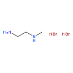
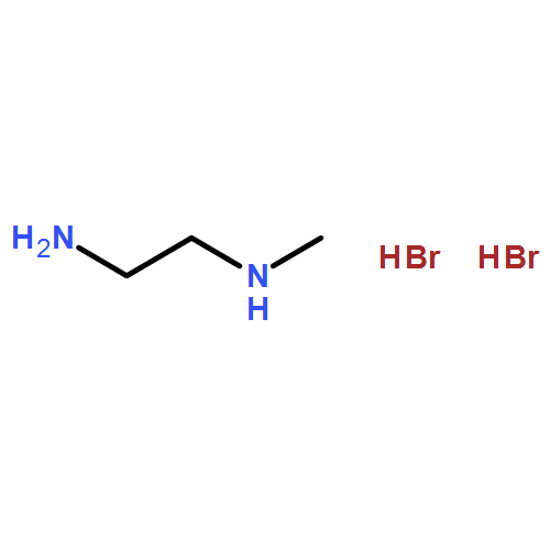
The recently discovered phenomenon of broadband white-light emission at room temperature in the (110) two-dimensional organic–inorganic perovskite (N-MEDA)[PbBr4] (N-MEDA = N1-methylethane-1,2-diammonium) is promising for applications in solid-state lighting. However, the spectral broadening mechanism and, in particular, the processes and dynamics associated with the emissive species are still unclear. Herein, we apply a suite of ultrafast spectroscopic probes to measure the primary events directly following photoexcitation, which allows us to resolve the evolution of light-induced emissive states associated with white-light emission at femtosecond resolution. Terahertz spectra show fast free carrier trapping and transient absorption spectra show the formation of self-trapped excitons on femtosecond time-scales. Emission-wavelength-dependent dynamics of the self-trapped exciton luminescence are observed, indicative of an energy distribution of photogenerated emissive states in the perovskite. Our results are consistent with photogenerated carriers self-trapped in a deformable lattice due to strong electron–phonon coupling, where permanent lattice defects and correlated self-trapped states lend further inhomogeneity to the excited-state potential energy surface.
Co-reporter:Adam Jaffe; Yu Lin; Wendy L. Mao
Journal of the American Chemical Society 2015 Volume 137(Issue 4) pp:1673-1678
Publication Date(Web):January 12, 2015
DOI:10.1021/ja512396m
Pressure-induced changes in the electronic structure of two-dimensional Cu-based materials have been a subject of intense study. In particular, the possibility of suppressing the Jahn–Teller distortion of d9 Cu centers with applied pressure has been debated over a number of decades. We studied the structural and electronic changes resulting from the application of pressures up to ca. 60 GPa on a two-dimensional copper(II)–chloride perovskite using diamond anvil cells (DACs), through a combination of in situ powder X-ray diffraction, electronic absorption and vibrational spectroscopy, dc resistivity measurements, and optical observations. Our measurements show that compression of this charge-transfer insulator initially yields a first-order structural phase transition at ca. 4 GPa similar to previous reports on other CuII–Cl perovskites, during which the originally translucent yellow solid turns red. Further compression induces a previously unreported phase transition at ca. 8 GPa and dramatic piezochromism from translucent red-orange to opaque black. Two-probe dc resistivity measurements conducted within the DAC show the first instance of appreciable conductivity in CuII–Cl perovskites. The conductivity increases by 5 orders of magnitude between 7 and 50 GPa, with a maximum measured conductivity of 2.9 × 10⁻⁴ S·cm–1 at 51.4 GPa. Electronic absorption spectroscopy and variable-temperature conductivity measurements indicate that the perovskite behaves as a 1.0 eV band-gap semiconductor at 39.7 GPa and has an activation energy for electronic conduction of 0.232(1) eV at 40.2 GPa. Remarkably, all these changes are reversible: the material reverts to a translucent yellow solid upon decompression, and ambient pressure powder X-ray diffraction data taken before and after compression up to 60 GPa show that the original structure is maintained with minimal hysteresis.
Co-reporter:D. Solis-Ibarra, I. C. Smith and H. I. Karunadasa
Chemical Science 2015 vol. 6(Issue 7) pp:4054-4059
Publication Date(Web):05 May 2015
DOI:10.1039/C5SC01135C
Reaction with halogen vapor allows us to post-synthetically exchange halides in both three- (3D) and two-dimensional (2D) organic–inorganic metal-halide perovskites. Films of 3D Pb–I perovskites cleanly convert to films of Pb–Br or Pb–Cl perovskites upon exposure to Br2 or Cl2 gas, respectively. This gas–solid reaction provides a simple method to produce the high-quality Pb–Br or Pb–Cl perovskite films required for optoelectronic applications. Reactivity with halogens can be extended to the organic layers in 2D metal-halide perovskites. Here, terminal alkene groups placed between the inorganic layers can capture Br2 gas through chemisorption to form dibromoalkanes. This reaction's selectivity for Br2 over I2 allows us to scrub Br2 to obtain high-purity I2 gas streams. We also observe unusual halogen transfer between the inorganic and organic layers within a single perovskite structure. Remarkably, the perovskite's crystallinity is retained during these massive structural rearrangements.
Co-reporter:Eric T. Hoke, Daniel J. Slotcavage, Emma R. Dohner, Andrea R. Bowring, Hemamala I. Karunadasa and Michael D. McGehee
Chemical Science 2015 vol. 6(Issue 1) pp:613-617
Publication Date(Web):04 Nov 2014
DOI:10.1039/C4SC03141E
We report on reversible, light-induced transformations in (CH3NH3)Pb(BrxI1−x)3. Photoluminescence (PL) spectra of these perovskites develop a new, red-shifted peak at 1.68 eV that grows in intensity under constant, 1-sun illumination in less than a minute. This is accompanied by an increase in sub-bandgap absorption at ∼1.7 eV, indicating the formation of luminescent trap states. Light soaking causes a splitting of X-ray diffraction (XRD) peaks, suggesting segregation into two crystalline phases. Surprisingly, these photo-induced changes are fully reversible; the XRD patterns and the PL and absorption spectra revert to their initial states after the materials are left for a few minutes in the dark. We speculate that photoexcitation may cause halide segregation into iodide-rich minority and bromide-enriched majority domains, the former acting as a recombination center trap. This instability may limit achievable voltages from some mixed-halide perovskite solar cells and could have implications for the photostability of halide perovskites used in optoelectronics.
Co-reporter:Adam Jaffe, Abraham Saldivar Valdes, and Hemamala I. Karunadasa
Chemistry of Materials 2015 Volume 27(Issue 10) pp:3568
Publication Date(Web):April 29, 2015
DOI:10.1021/acs.chemmater.5b00990
Co-reporter:Emma R. Dohner ; Eric T. Hoke
Journal of the American Chemical Society 2014 Volume 136(Issue 5) pp:1718-1721
Publication Date(Web):January 14, 2014
DOI:10.1021/ja411045r
We use organic cations to template the solution-state assembly of corrugated lead halide layers in bulk crystalline materials. These layered hybrids emit radiation across the entire visible spectrum upon ultraviolet excitation. They are promising as single-source white-light phosphors for use with ultraviolet light-emitting diodes in solid-state lighting devices. The broadband emission provides high color rendition and the chromaticity coordinates of the emission can be tuned through halide substitution. We have isolated materials that emit the “warm” white light sought for many indoor lighting applications as well as “cold” white light that approximates the visible region of the solar spectrum. Material syntheses are inexpensive and scalable and binding agents are not required for film deposition, eliminating problems of binder photodegradation. These well-defined and tunable structures provide a flexible platform for studying the rare phenomenon of intrinsic broadband emission from bulk materials.
Co-reporter:Emma R. Dohner ; Adam Jaffe ; Liam R. Bradshaw
Journal of the American Chemical Society 2014 Volume 136(Issue 38) pp:13154-13157
Publication Date(Web):August 27, 2014
DOI:10.1021/ja507086b
We report on the second family of layered perovskite white-light emitters with improved photoluminescence quantum efficiencies (PLQEs). Upon near-ultraviolet excitation, two new Pb–Cl and Pb–Br perovskites emit broadband “cold” and “warm” white light, respectively, with high color rendition. Emission from large, single crystals indicates an origin from the bulk material and not surface defect sites. The Pb–Br perovskite has a PLQE of 9%, which is undiminished after 3 months of continuous irradiation. Our mechanistic studies indicate that the emission has contributions from strong electron–phonon coupling in a deformable lattice and from a distribution of intrinsic trap states. These hybrids provide a tunable platform for combining the facile processability of organic materials with the structural definition of crystalline, inorganic solids.
Co-reporter:Adam Jaffe and Hemamala I. Karunadasa
Inorganic Chemistry 2014 Volume 53(Issue 13) pp:6494-6496
Publication Date(Web):June 11, 2014
DOI:10.1021/ic500860t
Atomic-scale integration of polyether molecules and copper(II) chloride layers in a two-dimensional perovskite affords, to the best of our knowledge, the first example of extended Li+ cycling in a metal chloride electrode. The hybrid can cycle over 200 times as a cathode in a lithium battery with an open-circuit voltage of 3.2 V. In contrast, CuCl2 alone or the precursors to the hybrid cannot be cycled in a lithium battery, demonstrating the importance of the layered, organic–inorganic architecture. This work shows that appropriate organic groups can enable Li+ cycling in inexpensive, nontoxic, metal halide electrodes, which is promising for large-scale applications.
Co-reporter:Ian C. Smith;Dr. Eric T. Hoke;Dr. Diego Solis-Ibarra; Michael D. McGehee; Hemamala I. Karunadasa
Angewandte Chemie International Edition 2014 Volume 53( Issue 42) pp:11232-11235
Publication Date(Web):
DOI:10.1002/anie.201406466
Abstract
Two-dimensional hybrid perovskites are used as absorbers in solar cells. Our first-generation devices containing (PEA)2(MA)2[Pb3I10] (1; PEA=C6H5(CH2)2NH3+, MA=CH3NH3+) show an open-circuit voltage of 1.18 V and a power conversion efficiency of 4.73 %. The layered structure allows for high-quality films to be deposited through spin coating and high-temperature annealing is not required for device fabrication. The 3D perovskite (MA)[PbI3] (2) has recently been identified as a promising absorber for solar cells. However, its instability to moisture requires anhydrous processing and operating conditions. Films of 1 are more moisture resistant than films of 2 and devices containing 1 can be fabricated under ambient humidity levels. The larger bandgap of the 2D structure is also suitable as the higher bandgap absorber in a dual-absorber tandem device. Compared to 2, the layered perovskite structure may offer greater tunability at the molecular level for material optimization.
Co-reporter:Dr. Diego Solis-Ibarra ; Hemamala I. Karunadasa
Angewandte Chemie 2014 Volume 126( Issue 4) pp:1057-1060
Publication Date(Web):
DOI:10.1002/ange.201309786
Abstract
The tools of synthetic chemistry allow us to fine-tune the reactivity of molecules at a level of precision not yet accessible with inorganic solids. We have investigated hybrids that couple molecules to the superior thermal and mechanical properties of solids. Herein we present, to the best of our knowledge, the first demonstration of reactivity between hybrid perovskites and substrates. Reaction with iodine vapor results in a remarkable expansion of these materials (up to 36 % in volume) where new covalent CI bonds are formed with retention of crystallinity. These hybrids also show unusual examples of reversible chemisorption. Here, solid-state interactions extend the lifetime of molecules that cannot be isolated in solution. We have tuned the half-lives of the iodinated structures from 3 h to 3 days. These nonporous hybrids drive substrate capture and controlled release through chemical reactivity. We illustrate the strengths of the hybrid by considering radioactive iodine capture.
Co-reporter:Ian C. Smith;Dr. Eric T. Hoke;Dr. Diego Solis-Ibarra; Michael D. McGehee; Hemamala I. Karunadasa
Angewandte Chemie 2014 Volume 126( Issue 42) pp:11414-11417
Publication Date(Web):
DOI:10.1002/ange.201406466
Abstract
Two-dimensional hybrid perovskites are used as absorbers in solar cells. Our first-generation devices containing (PEA)2(MA)2[Pb3I10] (1; PEA=C6H5(CH2)2NH3+, MA=CH3NH3+) show an open-circuit voltage of 1.18 V and a power conversion efficiency of 4.73 %. The layered structure allows for high-quality films to be deposited through spin coating and high-temperature annealing is not required for device fabrication. The 3D perovskite (MA)[PbI3] (2) has recently been identified as a promising absorber for solar cells. However, its instability to moisture requires anhydrous processing and operating conditions. Films of 1 are more moisture resistant than films of 2 and devices containing 1 can be fabricated under ambient humidity levels. The larger bandgap of the 2D structure is also suitable as the higher bandgap absorber in a dual-absorber tandem device. Compared to 2, the layered perovskite structure may offer greater tunability at the molecular level for material optimization.
Co-reporter:Dr. Diego Solis-Ibarra ; Hemamala I. Karunadasa
Angewandte Chemie International Edition 2014 Volume 53( Issue 4) pp:1039-1042
Publication Date(Web):
DOI:10.1002/anie.201309786
Abstract
The tools of synthetic chemistry allow us to fine-tune the reactivity of molecules at a level of precision not yet accessible with inorganic solids. We have investigated hybrids that couple molecules to the superior thermal and mechanical properties of solids. Herein we present, to the best of our knowledge, the first demonstration of reactivity between hybrid perovskites and substrates. Reaction with iodine vapor results in a remarkable expansion of these materials (up to 36 % in volume) where new covalent CI bonds are formed with retention of crystallinity. These hybrids also show unusual examples of reversible chemisorption. Here, solid-state interactions extend the lifetime of molecules that cannot be isolated in solution. We have tuned the half-lives of the iodinated structures from 3 h to 3 days. These nonporous hybrids drive substrate capture and controlled release through chemical reactivity. We illustrate the strengths of the hybrid by considering radioactive iodine capture.
Co-reporter:Matthew D. Smith, Laurent Pedesseau, Mikaël Kepenekian, Ian C. Smith, Claudine Katan, Jacky Even and Hemamala I. Karunadasa
Chemical Science (2010-Present) 2017 - vol. 8(Issue 3) pp:NaN1968-1968
Publication Date(Web):2016/11/10
DOI:10.1039/C6SC02848A
We show that post-synthetic small-molecule intercalation can significantly reduce the electronic confinement of 2D hybrid perovskites. Using a combined experimental and theoretical approach, we explain structural, optical, and electronic effects of intercalating highly polarizable molecules in layered perovskites designed to stabilize the intercalants. Polarizable molecules in the organic layers substantially alter the optical and electronic properties of the inorganic layers. By calculating the spatially resolved dielectric profiles of the organic and inorganic layers within the hybrid structure, we show that the intercalants afford organic layers that are more polarizable than the inorganic layers. This strategy reduces the confinement of excitons generated in the inorganic layers and affords the lowest exciton binding energy for an n = 1 perovskite of which we are aware. We also demonstrate a method for computationally evaluating the exciton's binding energy by solving the Bethe–Salpeter equation for the exciton, which includes an ab initio determination of the material's dielectric profile across organic and inorganic layers. This new semi-empirical method goes beyond the imprecise phenomenological approximation of abrupt dielectric-constant changes at the organic–inorganic interfaces. This work shows that incorporation of polarizable molecules in the organic layers, through intercalation or covalent attachment, is a viable strategy for tuning 2D perovskites towards mimicking the reduced electronic confinement and isotropic light absorption of 3D perovskites while maintaining the greater synthetic tunability of the layered architecture.
Co-reporter:D. Solis-Ibarra, I. C. Smith and H. I. Karunadasa
Chemical Science (2010-Present) 2015 - vol. 6(Issue 7) pp:NaN4059-4059
Publication Date(Web):2015/05/05
DOI:10.1039/C5SC01135C
Reaction with halogen vapor allows us to post-synthetically exchange halides in both three- (3D) and two-dimensional (2D) organic–inorganic metal-halide perovskites. Films of 3D Pb–I perovskites cleanly convert to films of Pb–Br or Pb–Cl perovskites upon exposure to Br2 or Cl2 gas, respectively. This gas–solid reaction provides a simple method to produce the high-quality Pb–Br or Pb–Cl perovskite films required for optoelectronic applications. Reactivity with halogens can be extended to the organic layers in 2D metal-halide perovskites. Here, terminal alkene groups placed between the inorganic layers can capture Br2 gas through chemisorption to form dibromoalkanes. This reaction's selectivity for Br2 over I2 allows us to scrub Br2 to obtain high-purity I2 gas streams. We also observe unusual halogen transfer between the inorganic and organic layers within a single perovskite structure. Remarkably, the perovskite's crystallinity is retained during these massive structural rearrangements.
Co-reporter:Eric T. Hoke, Daniel J. Slotcavage, Emma R. Dohner, Andrea R. Bowring, Hemamala I. Karunadasa and Michael D. McGehee
Chemical Science (2010-Present) 2015 - vol. 6(Issue 1) pp:NaN617-617
Publication Date(Web):2014/11/04
DOI:10.1039/C4SC03141E
We report on reversible, light-induced transformations in (CH3NH3)Pb(BrxI1−x)3. Photoluminescence (PL) spectra of these perovskites develop a new, red-shifted peak at 1.68 eV that grows in intensity under constant, 1-sun illumination in less than a minute. This is accompanied by an increase in sub-bandgap absorption at ∼1.7 eV, indicating the formation of luminescent trap states. Light soaking causes a splitting of X-ray diffraction (XRD) peaks, suggesting segregation into two crystalline phases. Surprisingly, these photo-induced changes are fully reversible; the XRD patterns and the PL and absorption spectra revert to their initial states after the materials are left for a few minutes in the dark. We speculate that photoexcitation may cause halide segregation into iodide-rich minority and bromide-enriched majority domains, the former acting as a recombination center trap. This instability may limit achievable voltages from some mixed-halide perovskite solar cells and could have implications for the photostability of halide perovskites used in optoelectronics.
Co-reporter:Matthew D. Smith, Adam Jaffe, Emma R. Dohner, Aaron M. Lindenberg and Hemamala I. Karunadasa
Chemical Science (2010-Present) 2017 - vol. 8(Issue 6) pp:NaN4504-4504
Publication Date(Web):2017/04/24
DOI:10.1039/C7SC01590A
Through structural and optical studies of a series of two-dimensional hybrid perovskites, we show that broadband emission upon near-ultraviolet excitation is common to (001) lead-bromide perovskites. Importantly, we find that the relative intensity of the broad emission correlates with increasing out-of-plane distortion of the Pb–(μ-Br)–Pb angle in the inorganic sheets. Temperature- and power-dependent photoluminescence data obtained on a representative (001) perovskite support an intrinsic origin to the broad emission from the bulk material, where photogenerated carriers cause excited-state lattice distortions mediated through electron–lattice coupling. In contrast, most inorganic phosphors contain extrinsic emissive dopants or emissive surface sites. The design rules established here could allow us to systematically optimize white-light emission from layered hybrid perovskites by fine-tuning the bulk crystal structure.