Co-reporter:Man Qiao, Yu Wang, Yafei Li, and Zhongfang Chen
The Journal of Physical Chemistry C May 4, 2017 Volume 121(Issue 17) pp:9627-9627
Publication Date(Web):April 8, 2017
DOI:10.1021/acs.jpcc.7b02413
By means of comprehensive density functional theory (DFT) computations, we designed a new two-dimensional (2D) structure of silicon, namely, tetra-silicene. In tetra-silicene, each silicon atom binds with four neighboring Si atoms to form a 2D network composed of only tetragons. Our DFT computations demonstrate that tetra-silicene is of rather high experimental feasibility, as indicated by its considerable cohesive energy, all positive modes in the phonon spectrum, and the well maintained structure after 10 ps first-principles molecular dynamics simulations at 500 K. Tetra-silicene has rather intriguing mechanical properties featured with unusual negative Poisson’s ratios. Remarkably, different from hexagonal silicene (hexa-silicene) which is semi-metallic without a band gap, tetra-silicene is semiconducting with an appreciable indirect band gap of 0.19 eV, and it has a considerable carrier mobility of 1639.07 cm2 V–1 s–1. Encouragingly, our simulations suggest that tetra-silicene can be flexibly produced from hexa-silicene via mechanical conversion. Once synthesized, tetra-silicene would find many important applications in electronics and mechanical devices.
Co-reporter:Feng Li;Yu Wang;Hong Wu;Zhifa Liu;Urs Aeberhard
Journal of Materials Chemistry C 2017 vol. 5(Issue 44) pp:11515-11521
Publication Date(Web):2017/11/16
DOI:10.1039/C7TC03363J
Designing new two-dimensional (2D) semiconductors with high carrier mobilities is highly desirable for material innovation, especially when the configuration has novel topological properties. Here, we proposed a first-principles-based design of a 2D crystal, namely a Be2N6 monolayer. In which, each N atom is shared by two neighboring N atoms and one Be atom, forming a novel moiety of benzene-like N6 rings. Rather than the instability of hexazine, the Be2N6 monolayer has a moderate cohesive energy, good kinetic and thermodynamic stability, due to the stabilization effect of the Be element by forming twelve classical two-centre–two-electron (2c–2e) σ-bonds and five multicenter 6c–2e π-bonds. There are ten π electrons in a unit cell, which satisfies the Hückel rule [4n + 2] (n = 2), indicating the Be2N6 monolayer aromaticity. As a result, the Be2N6 monolayer has an ultra-high mechanical strength of up to 200 J m−2. Particle-swarm optimization (PSO) computations reveal that a cyclo-N6-containing Be2N6 monolayer is the lowest-energy configuration in 2D forms with a stoichiometry of 1 : 3, and therefore could be synthesized experimentally. Furthermore, the Be2N6 monolayer is an indirect semiconductor with a band gap of 1.71 eV at the hybrid functional level, close to that of the bulk amorphous silicon ∼1.6 eV widely used in solar cells. At this point, the high electron mobility of up to ∼104 cm2 V−1 s−1 and visible-light absorption of ∼105 cm−1 are observed for the Be2N6 monolayer. If realized, it will not only enrich the knowledge of the bonding nature of nitrogen but could also have potential applications in electronics and optoelectronics.
Co-reporter:Gan Luo, Yu Wang, Yafei Li
Science Bulletin 2017 Volume 62, Issue 19(Volume 62, Issue 19) pp:
Publication Date(Web):15 October 2017
DOI:10.1016/j.scib.2017.08.015
The development of non-platinum (Pt) oxygen reduction reaction (ORR) catalysts with high activity and low cost is of great importance for large-scale commercialization of fuel cells. By means of density functional theory (DFT) computations, we theoretically identified that two-dimensional (2D) iron-porphyrin (Fe-Pp) sheet, in which the active Fe sites are distributed regularly and separately, is an appealing candidate. The pristine Fe-Pp sheet exhibits considerably high catalytic activity and four-electron selectivity for ORR. Especially, the adsorption of ORR intermediates on Fe-Pp sheet can be significantly weakened by the addition of axial cyanogen (CN) ligand, resulting in pronouncedly enhanced ORR activity. More interestingly, the d band center of CN attached Fe-Pp (Fe-Pp-CN) sheet can be further tuned by applying the external tensile or compressive strain, leading to an enhancement or suppression of ORR catalytic performance. In particular, under a small biaxial tensile strain of 2%, the ORR activity of Fe-Pp-CN sheet is even higher than that of Pt and reaches to the top of activity volcano. Our studies open new ways to design effective non-Pt ORR catalysts for fuel cell technology.
Co-reporter:Yu-Jia Tang;Yu Wang;Xiao-Li Wang;Shun-Li Li;Wei Huang;Long-Zhang Dong;Chun-Hui Liu;Ya-Fei Li;Ya-Qian Lan
Advanced Energy Materials 2016 Volume 6( Issue 12) pp:
Publication Date(Web):
DOI:10.1002/aenm.201600116
Facile design of low-cost and highly active catalysts from earth-abundant elements is favorable for the industrial application of water splitting. Here, a simple strategy to synthesize an ultrathin molybdenum disulfide/nitrogen-doped reduced graphene oxide (MoS2/N-RGO-180) nanocomposite with the enlarged interlayer spacing of 9.5 Å by a one-step hydrothermal method is reported. The synergistic effects between the layered MoS2 nanosheets and N-doped RGO films contribute to the high activity for hydrogen evolution reaction (HER). MoS2/N-RGO-180 exhibits the excellent catalytic activity with a low onset potential of −5 mV versus reversible hydrogen elelctrode (RHE), a small Tafel slope of 41.3 mV dec−1, a high exchange current density of 7.4 × 10⁻⁴ A cm−2, and good stability over 5 000 cycles under acidic conditions. The HER performance of MoS2/N-RGO-180 nanocomposite is superior to the most reported MoS2-based catalysts, especially its onset potential and exchange current density. In this work, a novel and simple method to the preparation of low-cost MoS2-based electrocatalysts with the extraordinary HER performance is presented.
Co-reporter:Feng Li, Xiuhong Liu, Yu Wang and Yafei Li
Journal of Materials Chemistry A 2016 vol. 4(Issue 11) pp:2155-2159
Publication Date(Web):17 Feb 2016
DOI:10.1039/C6TC00454G
Low-dimensional semiconducting materials with moderate band gaps as well as high carrier mobilities are highly sought for future application in microelectronics. By means of hybrid density functional theory computations, we predicted that a novel two-dimensional (2D) IV–VI material, namely germanium monosulfide (GeS) monolayer, is a rather desirable candidate. According to our computations, GeS monolayer is semiconducting with an indirect band gap of 2.34 eV, which can be effectively tuned by employing an external strain. Remarkably, the GeS monolayer has an electron mobility of 3680 cm2 V−1 s−1, which is much higher than that of MoS2 monolayer. Our computations also revealed that GeS monolayer is a stable structure and can be obtained by exfoliation or mechanical cleavage techniques. These findings render GeS monolayer a promising 2D material for applications in future microelectronics, and call for more research attention on 2D IV–VI materials.
Co-reporter:Xiuhong Liu, Yu Wang, Feng Li and Yafei Li
Physical Chemistry Chemical Physics 2016 vol. 18(Issue 21) pp:14638-14643
Publication Date(Web):05 May 2016
DOI:10.1039/C6CP01828A
By means of state-of-the-art density functional theory (DFT) computations, we systematically studied the structural, electronic, and optical properties of a novel two dimensional material, namely stanane (SnH). According to our computational results, stanane is semiconducting with a direct band gap of 1.00 eV, which can be flexibly tuned by applying an external strain. Remarkably, stanane has much higher electron and hole mobilities than those of a MoS2 monolayer at room temperature. Moreover, stanane has rather strong optical absorption in the visible as well as infrared regions of the solar spectrum. These results provide many useful insights for the wide application of stanane in electronics and optoelectronics.
Co-reporter:Feng Li and Yafei Li
Journal of Materials Chemistry A 2015 vol. 3(Issue 14) pp:3416-3421
Publication Date(Web):13 Feb 2015
DOI:10.1039/C5TC00013K
In this work, density functional theory computations with van der Waals (vdW) corrections revealed the existence of rather strong C–H⋯F–C hydrogen bonding between hydrofluorinated graphene (HGF) monolayers, which have Janus-like geometrics. Interestingly, the individual HGF monolayer is semiconducting with a direct energy gap of 2.82 eV while the HGF bilayer is metallic in its most stable stacking pattern. Especially, applying an external electric field can effectively open a band gap for HGF bilayer, and correspondingly cause a metallic-semiconducting transition. These results open up opportunities in fabricating electronic and optoelectronic devices based on HGF nanosheets, and call for more usage of the weak interactions for band structure engineering.
Co-reporter:Yafei Li, Bay Allen Pantoja, and Zhongfang Chen
Journal of Chemical Theory and Computation 2014 Volume 10(Issue 3) pp:1265-1271
Publication Date(Web):January 23, 2014
DOI:10.1021/ct401083c
Density functional theory (DFT) computations with van der Waals (vdw) correction revealed the existence of considerable Cδ+Fδ−···Cδ+Fδ− dipole–dipole interactions between two experimentally realized C4F monolayers. The dipole–dipole interactions induce a subtle interlayer polarization, which results in a significantly reduced band gap for C4F bilayer as compared to the individual C4F monolayer. With increasing the number of stacked layers, the band gap of C4F nanosheets can be further reduced, leading to a semiconducting–metallic transition. Moreover, the band gap of C4F nanosheets can be feasibly modulated by applying an external electric field. Our results provide new insights on taking advantage of nonbonding interactions to tune the electronic properties of graphene materials.
Co-reporter:Yafei Li and Zhongfang Chen
The Journal of Physical Chemistry C 2014 Volume 118(Issue 2) pp:1148-1154
Publication Date(Web):December 31, 2013
DOI:10.1021/jp411783q
Comprehensive density functional theory computations with van der Waals (vdW) correction demonstrated that there exists strong hydrogen bonding between two-dimensional (2D) germanane layers. Especially, germanane layers all have a direct band gap, irrespective of stacking pattern and thickness. The band gap of germanane bilayer can be flexibly reduced by applying an external electronic field (E-field), leading to a semiconducting-metallic transition, whereas the band gap of germanane monolayer is rather robust in response to E-field. In contrast, the band gaps of both germanane monolayer and bilayer can be reduced to zero when subjected to a biaxial tensile strain. These results provide many useful insights for the wide applications of germanane layers in electronics and optoelectronics.
Co-reporter:Yu Wang ; Yafei Li ;Zhongfang Chen
The Journal of Physical Chemistry C 2014 Volume 118(Issue 43) pp:25051-25056
Publication Date(Web):October 5, 2014
DOI:10.1021/jp5078328
The wide band gap of boron nitride (BN) materials has been a main bottleneck for their wide applications in electronics. In this work, by means of density functional theory (DFT) computations, we demonstrated that the band gaps of BN nanoribbons (BNNRs), with either zigzag or armchair edges, can be significantly reduced by C2H termination. The neighboring C2H terminal groups of BNNRs can covalently connect with each other, forming infinite carbon chains along the edges. The newly formed carbon chains introduce conjugated π edge states, which contribute to the band gap reduction of BNNRs. C2H termination can also result in higher carrier mobility for BNNRs. This simple strategy offers great opportunities for developing BNNR-based electronic devices.
Co-reporter:Dr. Yafei Li;Yunlong Liao;Dr. Zhongfang Chen
Angewandte Chemie International Edition 2014 Volume 53( Issue 28) pp:7248-7252
Publication Date(Web):
DOI:10.1002/anie.201403833
Abstract
The design of new materials is an important subject in order to attain new properties and applications, and it is of particular interest when some peculiar topological properties such as reduced dimensionality and rule-breaking chemical bonding are involved. In this work, we designed a novel two-dimensional (2D) inorganic material, namely Be2C monolayer, by comprehensive density functional theory (DFT) computations. In Be2C monolayer, each carbon atom binds to six Be atoms in an almost planar fashion, forming a quasi-planar hexacoordinate carbon (phC) moiety. Be2C monolayer has good stability and is the lowest-energy structure in 2D space confirmed by a global minima search based on the particle-swarm optimization (PSO) method. As a semiconductor with a direct medium band gap, Be2C monolayer is promising for applications in electronics and optoelectronics.
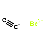
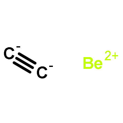
Co-reporter:Dr. Yafei Li;Yunlong Liao;Dr. Zhongfang Chen
Angewandte Chemie International Edition 2014 Volume 53( Issue 28) pp:
Publication Date(Web):
DOI:10.1002/anie.201405103
Co-reporter:Dr. Yafei Li;Yunlong Liao;Dr. Zhongfang Chen
Angewandte Chemie 2014 Volume 126( Issue 28) pp:7376-7380
Publication Date(Web):
DOI:10.1002/ange.201403833
Abstract
The design of new materials is an important subject in order to attain new properties and applications, and it is of particular interest when some peculiar topological properties such as reduced dimensionality and rule-breaking chemical bonding are involved. In this work, we designed a novel two-dimensional (2D) inorganic material, namely Be2C monolayer, by comprehensive density functional theory (DFT) computations. In Be2C monolayer, each carbon atom binds to six Be atoms in an almost planar fashion, forming a quasi-planar hexacoordinate carbon (phC) moiety. Be2C monolayer has good stability and is the lowest-energy structure in 2D space confirmed by a global minima search based on the particle-swarm optimization (PSO) method. As a semiconductor with a direct medium band gap, Be2C monolayer is promising for applications in electronics and optoelectronics.
Co-reporter:Dr. Yafei Li;Yunlong Liao;Dr. Zhongfang Chen
Angewandte Chemie 2014 Volume 126( Issue 28) pp:
Publication Date(Web):
DOI:10.1002/ange.201405103
Co-reporter:Xiuhong Liu, Yu Wang, Feng Li and Yafei Li
Physical Chemistry Chemical Physics 2016 - vol. 18(Issue 21) pp:NaN14643-14643
Publication Date(Web):2016/05/05
DOI:10.1039/C6CP01828A
By means of state-of-the-art density functional theory (DFT) computations, we systematically studied the structural, electronic, and optical properties of a novel two dimensional material, namely stanane (SnH). According to our computational results, stanane is semiconducting with a direct band gap of 1.00 eV, which can be flexibly tuned by applying an external strain. Remarkably, stanane has much higher electron and hole mobilities than those of a MoS2 monolayer at room temperature. Moreover, stanane has rather strong optical absorption in the visible as well as infrared regions of the solar spectrum. These results provide many useful insights for the wide application of stanane in electronics and optoelectronics.
Co-reporter:Feng Li and Yafei Li
Journal of Materials Chemistry A 2015 - vol. 3(Issue 14) pp:NaN3421-3421
Publication Date(Web):2015/02/13
DOI:10.1039/C5TC00013K
In this work, density functional theory computations with van der Waals (vdW) corrections revealed the existence of rather strong C–H⋯F–C hydrogen bonding between hydrofluorinated graphene (HGF) monolayers, which have Janus-like geometrics. Interestingly, the individual HGF monolayer is semiconducting with a direct energy gap of 2.82 eV while the HGF bilayer is metallic in its most stable stacking pattern. Especially, applying an external electric field can effectively open a band gap for HGF bilayer, and correspondingly cause a metallic-semiconducting transition. These results open up opportunities in fabricating electronic and optoelectronic devices based on HGF nanosheets, and call for more usage of the weak interactions for band structure engineering.
Co-reporter:Feng Li, Xiuhong Liu, Yu Wang and Yafei Li
Journal of Materials Chemistry A 2016 - vol. 4(Issue 11) pp:NaN2159-2159
Publication Date(Web):2016/02/17
DOI:10.1039/C6TC00454G
Low-dimensional semiconducting materials with moderate band gaps as well as high carrier mobilities are highly sought for future application in microelectronics. By means of hybrid density functional theory computations, we predicted that a novel two-dimensional (2D) IV–VI material, namely germanium monosulfide (GeS) monolayer, is a rather desirable candidate. According to our computations, GeS monolayer is semiconducting with an indirect band gap of 2.34 eV, which can be effectively tuned by employing an external strain. Remarkably, the GeS monolayer has an electron mobility of 3680 cm2 V−1 s−1, which is much higher than that of MoS2 monolayer. Our computations also revealed that GeS monolayer is a stable structure and can be obtained by exfoliation or mechanical cleavage techniques. These findings render GeS monolayer a promising 2D material for applications in future microelectronics, and call for more research attention on 2D IV–VI materials.