Co-reporter:Jun Feng, Xian Gong, Xiabing Lou, and Roy G. Gordon
ACS Applied Materials & Interfaces March 29, 2017 Volume 9(Issue 12) pp:10914-10914
Publication Date(Web):March 7, 2017
DOI:10.1021/acsami.7b01327
In advanced microelectronics, precise design of liner and capping layers become critical, especially when it comes to the fabrication of Cu interconnects with dimensions lower than its mean free path. Herein, we demonstrate that direct-liquid-evaporation chemical vapor deposition (DLE-CVD) of Co is a promising method to make liner and capping layers for nanoscale Cu interconnects. DLE-CVD makes pure, smooth, nanocrystalline, and highly conformal Co films with highly controllable growth characteristics. This process allows full Co encapsulation of nanoscale Cu interconnects, thus stabilizing Cu against diffusion and electromigration. Electrical measurements and high-resolution elemental imaging studies show that the DLE-CVD Co encapsulation layer can improve the reliability and thermal stability of Cu interconnects. Also, with the high conductivity of Co, the DLE-CVD Co encapsulation layer have the potential to further decrease the power consumption of nanoscale Cu interconnects, paving the way for Cu interconnects with higher efficiency in future high-end microelectronics.Keywords: cobalt; copper encapsulation; DLE-CVD; metal interconnect; nanocrystalline;
Co-reporter:Eugene S. Beh, Liuchuan Tong, and Roy G. Gordon
Organometallics April 24, 2017 Volume 36(Issue 8) pp:1453-1453
Publication Date(Web):April 6, 2017
DOI:10.1021/acs.organomet.6b00954
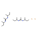
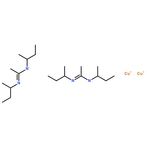
We describe the syntheses of three fully aliphatic 5,5-bicyclic amidines. The syntheses are facile and scalable and can be easily modified to produce other 5,5-bicyclic amidine ligands with other substitution patterns. Treatment of one of the ligands with KHMDS and subsequent transmetalation with CuCl resulted in a dimeric copper(I) bicyclic amidinate complex in 55% yield after recrystallization. This modestly air stable complex exhibits good volatility and thermal decomposition rates 1 order of magnitude lower than those of a similar, but acyclic, copper(I) amidinate. Together, the ligands enable a general method for producing a library of thermally stable metal amidinate precursors with a wide variety of metals for use in vapor deposition.
Co-reporter:Eugene S. BehDiana De Porcellinis, Rebecca L. Gracia, Kay T. Xia, Roy G. Gordon, Michael J. Aziz
ACS Energy Letters - New in 2016 2017 Volume 2(Issue 3) pp:
Publication Date(Web):February 7, 2017
DOI:10.1021/acsenergylett.7b00019
We demonstrate an aqueous organic and organometallic redox flow battery utilizing reactants composed of only earth-abundant elements and operating at neutral pH. The positive electrolyte contains bis((3-trimethylammonio)propyl)ferrocene dichloride, and the negative electrolyte contains bis(3-trimethylammonio)propyl viologen tetrachloride; these are separated by an anion-conducting membrane passing chloride ions. Bis(trimethylammoniopropyl) functionalization leads to ∼2 M solubility for both reactants, suppresses higher-order chemical decomposition pathways, and reduces reactant crossover rates through the membrane. Unprecedented cycling stability was achieved with capacity retention of 99.9943%/cycle and 99.90%/day at a 1.3 M reactant concentration, increasing to 99.9989%/cycle and 99.967%/day at 0.75–1.00 M; these represent the highest capacity retention rates reported to date versus time and versus cycle number. We discuss opportunities for future performance improvement, including chemical modification of a ferrocene center and reducing the membrane resistance without unacceptable increases in reactant crossover. This approach may provide the decadal lifetimes that enable organic–organometallic redox flow batteries to be cost-effective for grid-scale electricity storage, thereby enabling massive penetration of intermittent renewable electricity.
Co-reporter:Xiabing Lou, Hong Zhou, Sang Bok Kim, Sami Alghamdi, Xian Gong, Jun Feng, Xinwei Wang, Peide D. Ye, and Roy G. Gordon
Nano Letters 2016 Volume 16(Issue 12) pp:7650-7654
Publication Date(Web):November 28, 2016
DOI:10.1021/acs.nanolett.6b03638
We demonstrate for the first time that a single-crystalline epitaxial MgxCa1–xO film can be deposited on gallium nitride (GaN) by atomic layer deposition (ALD). By adjusting the ratio between the amounts of Mg and Ca in the film, a lattice matched MgxCa1–xO/GaN(0001) interface can be achieved with low interfacial defect density. High-resolution X-ray diffraction (XRD) shows that the lattice parameter of this ternary oxide nearly obeys Vegard’s law. An atomically sharp interface from cross-sectional transmission electron microscopy (TEM) confirmed the high quality of the epitaxy. High-temperature capacitance–voltage characterization showed that the film with composition Mg0.25Ca0.75O has the lowest interfacial defect density. With this optimal oxide composition, a Mg0.25Ca0.75O/AlGaN/GaN metal–oxide–semiconductor high-electron-mobility (MOS-HEMT) device was fabricated. An ultrahigh on/off ratio of 1012 and a near ideal SS of 62 mV/dec were achieved with this device.Keywords: dielectric; Epitaxy; GaN; magnesium calcium oxide; MOS-HEMT;
Co-reporter:Dr. Sang Bok Kim;Chuanxi Yang;Dr. Tamara Powers;Dr. Luke M. Davis;Xiabing Lou;Dr. Roy G. Gordon
Angewandte Chemie 2016 Volume 128( Issue 35) pp:
Publication Date(Web):
DOI:10.1002/ange.201683561
Co-reporter:Dr. Sang Bok Kim;Chuanxi Yang;Dr. Tamara Powers;Dr. Luke M. Davis;Xiabing Lou;Dr. Roy G. Gordon
Angewandte Chemie 2016 Volume 128( Issue 35) pp:10384-10389
Publication Date(Web):
DOI:10.1002/ange.201602406
Abstract
We have prepared two new CaII amidinates, which comprise a new class of ALD precursors. The syntheses proceed by a direct reaction between Ca metal and the amidine ligands in the presence of ammonia. Bis(N,N′-diisopropylformamidinato)calcium(II) (1) and bis(N,N′-diisopropylacetamidinato)calcium(II) (2) adopt dimeric structures in solution and in the solid state. X-ray crystallography revealed asymmetry in one of the bridging ligands to afford the structure [(η2-L)Ca(μ-η2:η2-L)(μ-η2:η1-L)Ca(η2-L)]. These amidinate complexes showed unprecedentedly high volatility as compared to the widely employed and commercially available CaII precursor, [Ca3(tmhd)6]. In CaS ALD with 1 and H2S, the ALD window was approximately two times wider and lower in temperature by about 150 °C than previously reported with [Ca3(tmhd)6] and H2S. Complexes 1 and 2, with their excellent volatility and thermal stability (up to at least 350 °C), are the first homoleptic CaII amidinates suitable for use as ALD precursors.
Co-reporter:Dr. Sang Bok Kim;Chuanxi Yang;Dr. Tamara Powers;Dr. Luke M. Davis;Xiabing Lou;Dr. Roy G. Gordon
Angewandte Chemie International Edition 2016 Volume 55( Issue 35) pp:10228-10233
Publication Date(Web):
DOI:10.1002/anie.201602406
Abstract
We have prepared two new CaII amidinates, which comprise a new class of ALD precursors. The syntheses proceed by a direct reaction between Ca metal and the amidine ligands in the presence of ammonia. Bis(N,N′-diisopropylformamidinato)calcium(II) (1) and bis(N,N′-diisopropylacetamidinato)calcium(II) (2) adopt dimeric structures in solution and in the solid state. X-ray crystallography revealed asymmetry in one of the bridging ligands to afford the structure [(η2-L)Ca(μ-η2:η2-L)(μ-η2:η1-L)Ca(η2-L)]. These amidinate complexes showed unprecedentedly high volatility as compared to the widely employed and commercially available CaII precursor, [Ca3(tmhd)6]. In CaS ALD with 1 and H2S, the ALD window was approximately two times wider and lower in temperature by about 150 °C than previously reported with [Ca3(tmhd)6] and H2S. Complexes 1 and 2, with their excellent volatility and thermal stability (up to at least 350 °C), are the first homoleptic CaII amidinates suitable for use as ALD precursors.
Co-reporter:Dr. Sang Bok Kim;Chuanxi Yang;Dr. Tamara Powers;Dr. Luke M. Davis;Xiabing Lou;Dr. Roy G. Gordon
Angewandte Chemie International Edition 2016 Volume 55( Issue 35) pp:
Publication Date(Web):
DOI:10.1002/anie.201683561
Co-reporter:Jing Yang, Kecheng Li, Jun Feng and Roy G. Gordon
Journal of Materials Chemistry A 2015 vol. 3(Issue 46) pp:12098-12106
Publication Date(Web):03 Nov 2015
DOI:10.1039/C5TC03221K
By a direct-liquid-evaporation chemical vapor deposition (DLE-CVD) method, we deposited smooth low-resistance cobalt (Co) and cobalt nitride (CoxN) thin films with excellent conformality at low temperatures down to 200 °C. In the DLE process, a cobalt amidinate precursor solution, bis(N,N′-diisopropylacetamidinato)cobalt(II) dissolved in tetradecane, was vaporized as it flowed smoothly, without boiling, inside heated tubing. This DLE process avoids creating unwanted particles that are generated when droplets from a nebulizer evaporate in a conventional direct-liquid-injection (DLI) process. The vapor then mixed with ammonia (NH3) and hydrogen (H2) and flowed over substrates in a tubular CVD reactor, resulting in metallic Co or CoxN films by tuning the NH3/H2 co-reactant ratio. This process deposited pure and highly conformal Co or CoxN films in trenches with 60:1 or 45:1 aspect ratio respectively. The good conformality is crucial towards realizing potential applications, such as in 3D contacts and interconnects in microelectronics.
Co-reporter:Kaixiang Lin;Qing Chen;Michael R. Gerhardt;Liuchuan Tong;Sang Bok Kim;Louise Eisenach;Alvaro W. Valle;David Hardee;Michael J. Aziz;Michael P. Marshak
Science 2015 Vol 349(6255) pp:1529-1532
Publication Date(Web):25 Sep 2015
DOI:10.1126/science.aab3033
A solution for scalable-flow batteries
Flow batteries, in which the redox active components are held in tanks separate from the active part of the cell, offer a scalable route for storing large quantities of energy. A challenge for their large-scale development is to avoid formulations that depend on toxic transition metal ions. Lin et al. show that quinones can be dissolved in alkaline solutions and coupled with ferricyanides to make a flow cell battery (see the Perspective by Perry). This gives scope for developing flow cells with very low costs, high efficiencies at practical power densities, simplicity of operation, and inherent safety.
Science, this issue p. 1529; see also p. 1452
Co-reporter:Yun Seog Lee;Danny Chua;Riley E. Brt;Sin Cheng Siah;Jian V. Li;Jonathan P. Mailoa;Sang Woon Lee;Tonio Buonassisi
Advanced Materials 2014 Volume 26( Issue 27) pp:4704-4710
Publication Date(Web):
DOI:10.1002/adma.201401054
Co-reporter:Sang Woon Lee;Yun Seog Lee;Jaeyeong Heo;Sin Cheng Siah;Danny Chua;Riley E. Brt;Sang Bok Kim;Jonathan P. Mailoa;Tonio Buonassisi
Advanced Energy Materials 2014 Volume 4( Issue 11) pp:
Publication Date(Web):
DOI:10.1002/aenm.201301916
Co-reporter:Prasert Sinsermsuksakul;Leizhi Sun;Sang Woon Lee;Helen Hejin Park;Sang Bok Kim;Chuanxi Yang
Advanced Energy Materials 2014 Volume 4( Issue 15) pp:
Publication Date(Web):
DOI:10.1002/aenm.201400496
Thin-film solar cells are made by vapor deposition of Earth-abundant materials: tin, zinc, oxygen and sulfur. These solar cells had previously achieved an efficiency of about 2%, less than 1/10 of their theoretical potential. Loss mechanisms are systematically investigated and mitigated in solar cells based on p-type tin monosulfide, SnS, absorber layers combined with n-type zinc oxysulfide, Zn(O,S) layers that selectively transmit electrons, but block holes. Recombination at grain boundaries is reduced by annealing the SnS films in H2S to form larger grains with fewer grain boundaries. Recombination near the p-SnS/n-Zn(O,S) junction is reduced by inserting a few monolayers of SnO2 between these layers. Recombination at the junction is also reduced by adjusting the conduction band offset by tuning the composition of the Zn(O,S), and by reducing its free electron concentration with nitrogen doping. The resulting cells have an efficiency over 4.4%, which is more than twice as large as the highest efficiency obtained previously by solar cells using SnS absorber layers.
Co-reporter:Sang Bok Kim, Prasert Sinsermsuksakul, Adam S. Hock, Robert D. Pike, and Roy G. Gordon
Chemistry of Materials 2014 Volume 26(Issue 10) pp:3065
Publication Date(Web):March 12, 2014
DOI:10.1021/cm403901y
Thin films containing germanium or tin have a great variety of current and potential applications, particularly their oxides or chalcogenides. Chemical vapor deposition (CVD) and atomic layer deposition (ALD) are popular ways to make these thin films conformally even on challenging nanostructured substrates. The success of these processes depends on having precursors that are sufficiently stable, volatile, and reactive. In this paper we optimize the syntheses of the following three precursors: 1 and 2 are racemic Ge(II) or Sn(II) cyclic amides made from N2,N3-di-tert-butylbutane-2,3-diamine, and 3 is bis(N,N′-diisopropylacetamidinato)tin(II). All three compounds are demonstrated to be effective precursors for ALD of their monosulfides, GeS or SnS, by reaction with H2S. 2 has also been reported previously to make polycrystalline SnO2 by ALD with oxidizing agents such as H2O2. The cyclic amides 1 and 2 are more volatile than the amidinate 3, vaporizing sufficiently for ALD even at precursor temperatures below 40 °C, whereas 3 vaporizes at temperatures over 90 °C. 1 and 2 can thus be used at lower substrate temperatures than 3. GeS or SnS can be deposited on substrates even at temperatures below 50 °C, while ALD of SnS from 3 becomes slow below substrate temperatures of 100 °C because of insufficient vapor pressure. The amount of growth per ALD cycle is higher for the cyclic amide 2 than for the amidinate 3. The GeS films are smooth and amorphous, while the SnS films are polycrystalline and granular. All of these films are uniformly thick inside holes with aspect ratios (depth/diameter) greater than 40:1.
Co-reporter:Xinwei Wang, Lin Dong, Jingyun Zhang, Yiqun Liu, Peide D. Ye, and Roy G. Gordon
Nano Letters 2013 Volume 13(Issue 2) pp:594-599
Publication Date(Web):December 31, 2012
DOI:10.1021/nl3041349
GaAs metal–oxide–semiconductor devices historically suffer from Fermi-level pinning, which is mainly due to the high trap density of states at the oxide/GaAs interface. In this work, we present a new way of passivating the interface trap states by growing an epitaxial layer of high-k dielectric oxide, La2–xYxO3, on GaAs(111)A. High-quality epitaxial La2–xYxO3 thin films are achieved by an ex situ atomic layer deposition (ALD) process, and GaAs MOS capacitors made from this epitaxial structure show very good interface quality with small frequency dispersion and low interface trap densities (Dit). In particular, the La2O3/GaAs interface, which has a lattice mismatch of only 0.04%, shows very low Dit in the GaAs bandgap, below 3 × 1011 cm–2 eV–1 near the conduction band edge. The La2O3/GaAs capacitors also show the lowest frequency dispersion of any dielectric on GaAs. This is the first achievement of such low trap densities for oxides on GaAs.
Co-reporter:Sang Woon Lee, Jaeyeong Heo and Roy G. Gordon
Nanoscale 2013 vol. 5(Issue 19) pp:8940-8944
Publication Date(Web):12 Aug 2013
DOI:10.1039/C3NR03082B
Recently, 2-dimensional electron gas (2-DEG) was discovered at the interface of Al2O3/SrTiO3 (STO) heterostructures, in which the amorphous Al2O3 layers were grown by atomic layer deposition (ALD). The saturated electron density at the Al2O3/STO heterostructures above the critical thickness of Al2O3 is explained by an oxygen diffusion mechanism.
Co-reporter:Xinwei Wang and Roy G. Gordon
Crystal Growth & Design 2013 Volume 13(Issue 3) pp:1316-1321
Publication Date(Web):February 1, 2013
DOI:10.1021/cg301801h
Pulsed chemical vapor deposition was used to prepare epitaxial ruthenium dioxide (RuO2) film on rutile TiO2 (011) at low temperature 280 °C. Reciprocal space mapping by high-resolution X-ray diffraction was used to examine the quality of epitaxy, which demonstrated a high quality epitaxy of the deposited RuO2 film. The results also showed that the RuO2 lattice was fully strained by the substrate in the lateral directions and, therefore, distorted from a tetragonal to a monoclinic structure.
Co-reporter:Sang Woon Lee, Yiqun Liu, Jaeyeong Heo, and Roy G. Gordon
Nano Letters 2012 Volume 12(Issue 9) pp:4775-4783
Publication Date(Web):August 21, 2012
DOI:10.1021/nl302214x
The formation of a two-dimensional electron gas (2-DEG) using SrTiO3 (STO)-based heterostructures provides promising opportunities in oxide electronics. We realized the formation of 2-DEG using several amorphous layers grown by the atomic layer deposition (ALD) technique at 300 °C which is a process compatible with mass production and thereby can provide the realization of potential applications. We found that the amorphous LaAlO3 (LAO) layer grown by the ALD process can generate 2-DEG (∼1 × 10¹³/cm2) with an electron mobility of 4–5 cm2/V·s. A much higher electron mobility was observed at lower temperatures. More remarkably, amorphous YAlO3 (YAO) and Al2O3 layers, which are not polar-perovskite-structured oxides, can create 2-DEG as well. 2-DEG was created by means of the important role of trimethylaluminum, Me3Al, as a reducing agent for STO during LAO and YAO ALD as well as the Al2O3 ALD process at 300 °C. The deposited oxide layer also plays an essential role as a catalyst that enables Me3Al to reduce the STO. The electrons were localized very near to the STO surface, and the source of carriers was explained based on the oxygen vacancies generated in the STO substrate.
Co-reporter:Ho-Jin Son ; Xinwei Wang ; Chaiya Prasittichai ; Nak Cheon Jeong ; Titta Aaltonen ; Roy G. Gordon ;Joseph T. Hupp
Journal of the American Chemical Society 2012 Volume 134(Issue 23) pp:9537-9540
Publication Date(Web):June 1, 2012
DOI:10.1021/ja300015n
A major loss mechanism in dye-sensitized solar cells (DSCs) is recombination at the TiO2/electrolyte interface. Here we report a method to reduce greatly this loss mechanism. We deposit insulating and transparent silica (SiO2) onto the open areas of a nanoparticulate TiO2 surface while avoiding any deposition of SiO2 over or under the organic dye molecules. The SiO2 coating covers the highly convoluted surface of the TiO2 conformally and with a uniform thickness throughout the thousands of layers of nanoparticles. DSCs incorporating these selective and self-aligned SiO2 layers achieved a 36% increase in relative efficiency versus control uncoated cells.
Co-reporter:Prasert Sinsermsuksakul, Rupak Chakraborty, Sang Bok Kim, Steven M. Heald, Tonio Buonassisi, and Roy G. Gordon
Chemistry of Materials 2012 Volume 24(Issue 23) pp:4556
Publication Date(Web):November 15, 2012
DOI:10.1021/cm3024988
Thin-film solar cells made from earth-abundant, inexpensive, and nontoxic materials are needed to replace the current technologies whose widespread use is limited by their use of scarce, costly, and toxic elements.(1) Tin monosulfide (SnS) is a promising candidate for making absorber layers in scalable, inexpensive, and nontoxic solar cells. SnS has always been observed to be a p-type semiconductor. Doping SnS to form an n-type semiconductor would permit the construction of solar cells with p-n homojunctions. This paper reports doping SnS films with antimony, a potential n-type dopant. Small amounts of antimony (∼1%) were found to greatly increase the electrical resistance of the SnS. The resulting intrinsic SnS(Sb) films could be used for the insulating layer in a p-i-n design for solar cells. Higher concentrations (∼5%) of antimony did not convert the SnS(Sb) to low-resistivity n-type conductivity, but instead the films retain such a high resistance that the conductivity type could not be determined. Extended X-ray absorption fine structure analysis reveals that the highly doped films contain precipitates of a secondary phase that has chemical bonds characteristic of metallic antimony, rather than the antimony–sulfur bonds found in films with lower concentrations of antimony.Keywords: antimony; doping; semiconductor; thin films; tin sulfide;
Co-reporter:Jaeyeong Heo, Sang Bok Kim and Roy G. Gordon
Journal of Materials Chemistry A 2012 vol. 22(Issue 11) pp:4599-4602
Publication Date(Web):03 Feb 2012
DOI:10.1039/C2JM16557K
Atomic layer deposition (ALD) of tin oxide (SnO2) thin films was achieved using a cyclic amide of Sn(II) (1,3-bis(1,1-dimethylethyl)-4,5-dimethyl-(4R,5R)-1,3,2-diazastannolidin-2-ylidene) as a tin precursor and nitric oxide (NO) as an oxidant gas. Film properties as a function of growth temperature from 130–250 °C were studied. Highly conducting SnO2 films were obtained at 200–250 °C with the growth per cycle of ∼1.4 Å/cycle, while insulating films were grown at temperatures lower than 200 °C. Conformal growth of SnO2 in holes of aspect-ratios up to ∼50:1 was successfully demonstrated.
Co-reporter:Prasert Sinsermsuksakul;Jaeyeong Heo;Wontae Noh;Adam S. Hock
Advanced Energy Materials 2011 Volume 1( Issue 6) pp:1116-1125
Publication Date(Web):
DOI:10.1002/aenm.201100330
Abstract
Thin film solar cells made from earth-abundant, non-toxic materials are needed to replace the current technology that uses Cu(In,Ga)(S,Se)2 and CdTe, which contain scarce and toxic elements. One promising candidate absorber material is tin monosulfide (SnS). In this report, pure, stoichiometric, single-phase SnS films were obtained by atomic layer deposition (ALD) using the reaction of bis(N,N′-diisopropylacetamidinato)tin(II) [Sn(MeC(N-iPr)2)2] and hydrogen sulfide (H2S) at low temperatures (100 to 200 °C). The direct optical band gap of SnS is around 1.3 eV and strong optical absorption (α > 104 cm−1) is observed throughout the visible and near-infrared spectral regions. The films are p-type semiconductors with carrier concentration on the order of 1016 cm−3 and hole mobility 0.82–15.3 cm2V−1s−1 in the plane of the films. The electrical properties are anisotropic, with three times higher mobility in the direction through the film, compared to the in-plane direction.
Co-reporter:Jaeyeong Heo ; Yiqun Liu ; Prasert Sinsermsuksakul ; Zhefeng Li ; Leizhi Sun ; Wontae Noh
The Journal of Physical Chemistry C 2011 Volume 115(Issue 20) pp:10277-10283
Publication Date(Web):April 28, 2011
DOI:10.1021/jp202202x
(Sn,Al)Ox composite films with various aluminum (Al) to tin (Sn) ratios were deposited using an atomic layer deposition technique. The chemisorption behavior of cyclic amide of tin(II) and trimethylaluminum were analyzed by Rutherford backscattering spectroscopy. Both precursors showed retarded and enhanced chemisorption on Al2O3 and SnO2 surfaces, respectively. The films show highly anisotropic electrical conductivity, i.e., much higher resistivity in the direction through the film than parallel to the surface of the film. The cause of the anisotropy was investigated by cross-sectional transmission electron microscopy, which showed a nanolaminate structure of crystalline SnO2 grains separated by thin, amorphous Al2O3 monolayers. When the Al concentration was higher than ∼35 atom %, the composite films became amorphous, and the vertical and lateral direction resistivity values converged toward one value. By properly choosing the ratio of SnO2 and Al2O3 subcycles, controlled adjustment of film electrical resistivity over more than 15 orders of magnitude was successfully demonstrated.
Co-reporter:Zhefeng Li, Roy G. Gordon, Venkateswara Pallem, Huazhi Li and Deo V. Shenai
Chemistry of Materials 2010 Volume 22(Issue 10) pp:3060
Publication Date(Web):April 27, 2010
DOI:10.1021/cm903636j
Smooth and continuous films of nickel nitride (NiNx) with excellent step coverage were deposited from a novel nickel amidinate precursor, Ni(MeC(NtBu)2)2, and either ammonia (NH3) or a mixture of NH3 and hydrogen (H2) gases as co-reactants. The reactants were injected together in direct-liquid-injection chemical vapor deposition (DLI-CVD) processes at substrate temperatures of 160−200 °C. Depending on the ratio of NH3 to H2 gases during deposition, the Ni:N atomic ratio in DLI-CVD NiNx films could be varied from ∼3:1 to ∼15:1, having either a cubic nickel structure or a mixture of hexagonal Ni3N and cubic Ni4N crystal structures with an incorporation of nitrogen as low as 6%. The chemical vapor deposition (CVD) growth rates of NiNx could be increased to more than 5 nm/min. The CVD films were smooth and continuous, and they had ∼100% step coverage in high-aspect-ratio (>50:1) holes. The as-deposited NiNx films had resistivities as low as ∼50 μΩ cm for film thicknesses of ∼25 nm. Annealing of the films in H2 at 160 °C or hydrogen plasma treatment at room temperature removed the nitrogen and led to pure nickel films.
Co-reporter:Jaeyeong Heo, Adam S. Hock and Roy G. Gordon
Chemistry of Materials 2010 Volume 22(Issue 17) pp:4964
Publication Date(Web):August 11, 2010
DOI:10.1021/cm1011108
Atomic layer deposition (ALD) of tin oxide (SnOx) films was achieved using a newly synthesized tin precursor and hydrogen peroxide. We obtained highly pure, conductive SnOx films at temperatures as low as 50 °C, which was possible because of high chemical reactivity between the new Sn precursor and hydrogen peroxide. The growth per cycle is around 0.18 nm/cycle in the ALD window up to 150 °C, and decreased at higher temperatures. Self-limited growth was demonstrated for both the Sn and O precursors. Thickness is linear in the number of cycles, with an induction period of not more than a few cycles. Rutherford backscattering spectroscopy (RBS) and X-ray photoelectron spectroscopy (XPS) measurements showed that the composition ratio of O/Sn is ∼2 and that the films do not contain any detectable carbon or nitrogen impurities. X-ray and electron diffraction analyses identified crystallites of SnO2 with the rutile structure and average grain size 5−10 nm. The density of the films is 83% of the bulk rutile phase. The surfaces are very smooth, with roughness about 3% of the film thickness. The lowest resistivity is about 10−2 ohm·cm. The mobility is over 7 cm2/V·s, and the free electron concentration reaches nearly 1020 cm−3. The dependence of mobility on temperature suggests that grain boundary scattering is the dominant electron scattering mechanism. The optical transmission of a 100 nm film is 87.8% and its absorption is 3.3% when averaged over the wavelengths from 400 to 800 nm. Over 80% uniformity of thickness was achieved inside holes with aspect ratios up to 50:1. This successful low temperature growth of conductive nanocrystalline SnOx films by ALD allows it to be exploited in transparent electrodes for displays, organic light emitting diodes, solar cells, conductive and protective coatings on plastic, microchannel electron multiplier plates, or as a semiconductor layer in transparent transistors.
Co-reporter:Hongtao Wang;Roger Alvis;Robert M. Ulfig
Chemical Vapor Deposition 2009 Volume 15( Issue 10-12) pp:312-319
Publication Date(Web):
DOI:10.1002/cvde.200906789
Abstract
Ruthenium thin films are deposited by atomic layer deposition (ALD) from bis(N,N'-di-tert-butylacetamidinato)ruthenium(II) dicarbonyl and O2. Highly conductive, dense, and pure thin films can be deposited when oxygen exposure, EO, approaches a certain threshold (Emax). When EO > Emax the film peels off due to the recombinative desorption of O2 at the film/substrate interface. Analysis by atomic probe microscopy (APM) shows that the crystallites are nearly free from carbon impurity (<0.1 at.-%), while a low level of carbon (<0.5 at.-%) is segregated near the grain boundaries. APM also shows that a small amount of O impurity (0.3 at.-%) is distributed uniformly between the crystallites and the grain boundaries.
Co-reporter:Zhengwen Li, Don Kuen Lee, Michael Coulter, Leonard N. J. Rodriguez and Roy G. Gordon
Dalton Transactions 2008 (Issue 19) pp:2592-2597
Publication Date(Web):14 Apr 2008
DOI:10.1039/B800712H
Three new volatile cobalt amidinate compounds were prepared: Co(tBuNC(R)NEt)2, R = Me, Et and n-Bu. They were characterized by elemental analysis, 1H NMR, X-ray structure analysis, melting point, vapor pressure, vaporization rate, thermal stability and chemical reactivity. They were found to evaporate cleanly without decomposition. Two of them are liquids at room temperature, allowing for more convenient preparation, handling and purification by distillation. They are highly reactive compounds that have been found to be suitable precursors for vapor deposition of cobalt metal, cobalt nitride and cobalt oxide. A new synthetic method allows for the facile and inexpensive preparation of large quantities of these compounds.
Co-reporter:Xin-Gui Li;Zhengwen Li;Huazhi Li
European Journal of Inorganic Chemistry 2007 Volume 2007(Issue 8) pp:
Publication Date(Web):9 FEB 2007
DOI:10.1002/ejic.200600960
A highly volatile asymmetric iron(II) amidinate, iron(II) bis(N-tert-butyl-N′-ethylacetamidinate), was synthesized for the first time by systematically changing starting iron(II) compounds such as acetylacetonate, acetate, and chloride, in different media such as diethyl ether, toluene, and tetrahydrofuran. The amidinate has been characterized and compared with the symmetric iron(II) bis(N,N′-diisopropylacetamidinate) by NMR spectroscopy, MS, IR spectroscopy, and dynamic and isothermal thermogravimetric techniques. Different amidinates from three starting compounds exhibit almost the same NMR, MS, and IR spectra, a melting point of 85 °C, and the same solution color in the same solvents, but quite different synthetic yields, volatilities, and colors in different solvents. This implies that the amidinates show an interesting solvatochromism. In particular, the asymmetric iron(II) amidinates obtained should be a mixture of paramagnetic and diamagnetic compounds. The thermostability and sublimation kinetics of the iron(II) amidinates have been investigated in detail. It is found that the average activation energy of 106 kJ mol–1 for the nonisothermal sublimation is slightly higher than the average activation energy of 104 kJ mol–1 determined from the isothermal thermogravimetric experiments. The sublimation is a diffusion-controlled process because the temperature and the rate of the sublimation depend strongly on the sublimation level and the sample size. The optimal iron(II) starting compound and reaction medium should be iron(II) acetylacetonate and diethyl ether, respectively, because the combination offers the highest yield, the greatest volatilizability of 98 %, and thus the purest product. (© Wiley-VCH Verlag GmbH & Co. KGaA, 69451 Weinheim, Germany, 2007)
Co-reporter:Z. Li;R. G. Gordon
Chemical Vapor Deposition 2006 Volume 12(Issue 7) pp:
Publication Date(Web):6 JUL 2006
DOI:10.1002/cvde.200606485
Thin and continuous copper films serve as seed layers for electrodeposition of interconnects in microelectronic devices. Gaps in the continuity of these Cu films must be avoided, because they can generate voids that later lead to failure of the devices. It is difficult to sputter completely continuous copper-seed layers into the increasingly narrow trenches and holes in modern interconnects. Here we report a method for producing thin, completely continuous, and highly conductive copper films conformally inside very narrow holes with aspect ratios of over 40:1. The first step in our process is atomic layer deposition (ALD) of copper(I) nitride, Cu3N, by the alternating reactions of copper(I) N,N′-di-sec-butylacetamidinate vapor and ammonia on surfaces heated to approximately 160 °C. At this temperature, Cu3N is thermally stable, but is readily reduced to copper metal by exposure to molecular hydrogen gas (H2). Copper layers as thin as 0.8 nm (about 3 monolayers) are electrically continuous and show the electrical resistivity predicted by a grain-boundary-scattering model for continuous films of that thickness. 3 nm thick copper films on 2 nm of ruthenium have a sheet resistance of less than 50 Ω/□, a value low enough to serve as seed layers for advanced electroplating techniques.
Co-reporter:P. de Rouffignac;R. G. Gordon
Chemical Vapor Deposition 2006 Volume 12(Issue 2-3) pp:
Publication Date(Web):22 MAR 2006
DOI:10.1002/cvde.200506377
Praseodymium aluminum oxide (PAO) thin films were grown by atomic layer deposition (ALD) from a new precursor, tris(N,N′-diisopropylacetamidinato) praseodymium, (Pr(amd)3), trimethylaluminum (TMA), and water. Smooth, amorphous films having varying compositions of the general formula PrxAl2–xO3 were deposited on HF-last silicon and analyzed for physical and electrical characteristics. The films were pure according to Rutherford backscattering spectrometry (RBS) and secondary ion mass spectrometry (SIMS). The permittivity of the thin film with the stoichiometry of Pr1.15Al0.85O3 was 18, and all annealed films displayed very low leakage currents compared to other high-k oxide films deposited using ALD. A leakage current density of 1.1 × 10⁻⁴ A cm–2 was achieved for a PAO film with an equivalent oxide thickness of 1.46 nm. Annealed films also displayed nearly zero flat-band voltage shifts and low hysteresis (< 10 mV). The optimal growth parameters and electrical properties were achieved with Pr1.15Al0.85O3. Atomic force microscopy (AFM) determined that high temperature annealing (850 °C) had no effect on the smoothness of the films (rms of 0.17 nm).
Co-reporter:Roy G. Gordon, Seán Barry, Jeffrey T. Barton, Randy N.R. Broomhall-Dillard
Thin Solid Films 2001 Volume 392(Issue 2) pp:231-235
Publication Date(Web):30 July 2001
DOI:10.1016/S0040-6090(01)01033-1
Tungsten oxide, WOx, is a coloring layer commonly used in electrochromic windows and displays. Successful commercialization of these devices will require the deposition of WOx layers with extremely uniform thickness and material properties over large areas at high speeds and low cost. We present a new atmospheric pressure chemical vapor deposition process that should be able to meet these goals. New liquid tungsten precursors have been found to have properties suitable for this application: sufficient volatility, reactivity to oxygen at substrate temperatures of 200–300°C, lack of reactivity to air and water at room temperature, and low viscosity (7 centiPoise at 40°C). The precursors are tungsten pentacarbonyl 1-methylbutylisonitrile and tungsten pentacarbonyl n-pentylisonitrile, C5H11NCW(CO)5. These liquid precursors can be synthesized readily from commercially available reactants. Data on the composition and structure of the tungsten oxide films are presented, along with spectroscopic characterization of the films in transparent (oxidized) and colored (reduced) states.
Co-reporter:Jaeyeong Heo, Sang Bok Kim and Roy G. Gordon
Journal of Materials Chemistry A 2012 - vol. 22(Issue 11) pp:NaN4602-4602
Publication Date(Web):2012/02/03
DOI:10.1039/C2JM16557K
Atomic layer deposition (ALD) of tin oxide (SnO2) thin films was achieved using a cyclic amide of Sn(II) (1,3-bis(1,1-dimethylethyl)-4,5-dimethyl-(4R,5R)-1,3,2-diazastannolidin-2-ylidene) as a tin precursor and nitric oxide (NO) as an oxidant gas. Film properties as a function of growth temperature from 130–250 °C were studied. Highly conducting SnO2 films were obtained at 200–250 °C with the growth per cycle of ∼1.4 Å/cycle, while insulating films were grown at temperatures lower than 200 °C. Conformal growth of SnO2 in holes of aspect-ratios up to ∼50:1 was successfully demonstrated.
Co-reporter:Jing Yang, Kecheng Li, Jun Feng and Roy G. Gordon
Journal of Materials Chemistry A 2015 - vol. 3(Issue 46) pp:NaN12106-12106
Publication Date(Web):2015/11/03
DOI:10.1039/C5TC03221K
By a direct-liquid-evaporation chemical vapor deposition (DLE-CVD) method, we deposited smooth low-resistance cobalt (Co) and cobalt nitride (CoxN) thin films with excellent conformality at low temperatures down to 200 °C. In the DLE process, a cobalt amidinate precursor solution, bis(N,N′-diisopropylacetamidinato)cobalt(II) dissolved in tetradecane, was vaporized as it flowed smoothly, without boiling, inside heated tubing. This DLE process avoids creating unwanted particles that are generated when droplets from a nebulizer evaporate in a conventional direct-liquid-injection (DLI) process. The vapor then mixed with ammonia (NH3) and hydrogen (H2) and flowed over substrates in a tubular CVD reactor, resulting in metallic Co or CoxN films by tuning the NH3/H2 co-reactant ratio. This process deposited pure and highly conformal Co or CoxN films in trenches with 60:1 or 45:1 aspect ratio respectively. The good conformality is crucial towards realizing potential applications, such as in 3D contacts and interconnects in microelectronics.

![4,4'-Bipyridinium, 1,1'-bis[3-(trimethylammonio)propyl]-, tetrachloride](http://img.cochemist.com/ccimg/108300/108228-37-1.png)
![4,4'-Bipyridinium, 1,1'-bis[3-(trimethylammonio)propyl]-, tetrachloride](http://img.cochemist.com/ccimg/108300/108228-37-1_b.png)