Co-reporter:Ute Zschieschang, Vera Patricia Bader, Hagen Klauk
Organic Electronics 2017 Volume 49(Volume 49) pp:
Publication Date(Web):1 October 2017
DOI:10.1016/j.orgel.2017.06.045
•Flexible p- and n-channel organic TFTs with on/off ratios of 2 × 10⁵ for gate-source voltages between 0 and 0.7 V are shown.•Complementary inverters have a gain of 90 and a minimum noise margin of 79% when operated with a supply voltage of 0.7 V.•Complementary ring oscillators can be operated with supply voltages as small as 0.4 V.In many of the applications envisioned for organic thin-film transistors (TFTs), the electrical power will be supplied by small batteries or energy harvesters, which implies that it will be beneficial if the TFTs can be operated with voltages of 1 V or even below 1 V. At the same time, the TFTs should have large on/off current ratios, especially for applications in digital circuits and active matrices. Here we demonstrate p-channel and n-channel organic TFTs fabricated on a flexible plastic substrate that have a turn-on voltage of exactly 0 V, a subthreshold slope of 100 mV/decade, and an on/off current ratio of 2 × 10⁵ when operated with gate-source voltages between 0 and 0.7 V. Complementary inverters fabricated using these TFTs have a small-signal gain of 90 and a minimum noise margin of 79% at a supply voltage of 0.7 V. Complementary ring oscillators can be operated with supply voltages as small as 0.4 V.Download high-res image (285KB)Download full-size image
Co-reporter:Mahdieh Aghamohammadi, Reinhold Rödel, Ute Zschieschang, Carmen Ocal, Hans Boschker, R. Thomas Weitz, Esther Barrena, and Hagen Klauk
ACS Applied Materials & Interfaces 2015 Volume 7(Issue 41) pp:22775
Publication Date(Web):September 28, 2015
DOI:10.1021/acsami.5b02747
The mechanisms behind the threshold-voltage shift in organic transistors due to functionalizing of the gate dielectric with self-assembled monolayers (SAMs) are still under debate. We address the mechanisms by which SAMs determine the threshold voltage, by analyzing whether the threshold voltage depends on the gate-dielectric capacitance. We have investigated transistors based on five oxide thicknesses and two SAMs with rather diverse chemical properties, using the benchmark organic semiconductor dinaphtho[2,3-b:2′,3′-f]thieno[3,2-b]thiophene. Unlike several previous studies, we have found that the dependence of the threshold voltage on the gate-dielectric capacitance is completely different for the two SAMs. In transistors with an alkyl SAM, the threshold voltage does not depend on the gate-dielectric capacitance and is determined mainly by the dipolar character of the SAM, whereas in transistors with a fluoroalkyl SAM the threshold voltages exhibit a linear dependence on the inverse of the gate-dielectric capacitance. Kelvin probe force microscopy measurements indicate this behavior is attributed to an electronic coupling between the fluoroalkyl SAM and the organic semiconductor.Keywords: gate-dielectric capacitance; Kelvin probe force microscopy; organic transistors; self-assembled monolayers; threshold-voltage shift
Co-reporter:Daniel Kälblein, Hyeyeon Ryu, Frederik Ante, Bernhard Fenk, Kersten Hahn, Klaus Kern, and Hagen Klauk
ACS Nano 2014 Volume 8(Issue 7) pp:6840
Publication Date(Web):June 18, 2014
DOI:10.1021/nn501484e
A method for the formation of a low-temperature hybrid gate dielectric for high-performance, top-gate ZnO nanowire transistors is reported. The hybrid gate dielectric consists of a self-assembled monolayer (SAM) and an aluminum oxide layer. The thin aluminum oxide layer forms naturally and spontaneously when the aluminum gate electrode is deposited by thermal evaporation onto the SAM-covered ZnO nanowire, and its formation is facilitated by the poor surface wetting of the aluminum on the hydrophobic SAM. The hybrid gate dielectric shows excellent electrical insulation and can sustain voltages up to 6 V. ZnO nanowire transistors utilizing the hybrid gate dielectric feature a large transconductance of 50 μS and large on-state currents of up to 200 μA at gate-source voltages of 3 V. The large on-state current is sufficient to drive organic light-emitting diodes with an active area of 6.7 mm2 to a brightness of 445 cd/m2. Inverters based on ZnO nanowire transistors and thin-film carbon load resistors operate with frequencies up to 30 MHz.Keywords: hybrid dielectric; nanowire transistors; organic light-emitting diodes; zinc oxide
Co-reporter:Sonja Geib;Ute Zschieschang;Marcel Gsänger;Matthias Stolte;Frank Würthner;Hubert Wadepohl;Lutz H. Gade
Advanced Functional Materials 2013 Volume 23( Issue 31) pp:3866-3874
Publication Date(Web):
DOI:10.1002/adfm.201203600
Abstract
Organic thin-film transistors (TFTs) are prepared by vacuum deposition and solution shearing of 2,9-bis(perfluoroalkyl)-substituted tetraazaperopyrenes (TAPPs) with bromine substituents at the aromatic core. The TAPP derivatives are synthesized by reacting known unsubstituted TAPPs with bromine in fuming sulphuric acid, and their electrochemical properties are studied in detail by cyclic voltammetry and modelled with density functional theory (DFT) methods. Lowest unoccupied molecular orbital (LUMO) energies and electron affinities indicate that the core-brominated TAPPs should exhibit n-channel semiconducting properties. Current-voltage characteristics of the TFTs established electron mobilities of up to μn = 0.032 cm2 V−1 s−1 for a derivative which was subsequently processed in the fabrication of a complementary ring oscillator on a flexible plastic substrate (PEN).
Co-reporter:Robert Hofmockel, Ute Zschieschang, Ulrike Kraft, Reinhold Rödel, Nis Hauke Hansen, Matthias Stolte, Frank Würthner, Kazuo Takimiya, Klaus Kern, Jens Pflaum, Hagen Klauk
Organic Electronics 2013 Volume 14(Issue 12) pp:3213-3221
Publication Date(Web):December 2013
DOI:10.1016/j.orgel.2013.09.003
•Organic thin-film transistors based on the small-molecule semiconductor C10-DNTT are fabricated.•TFTs with a vacuum-deposited semiconductor layer have hole mobilities up to 8.5 cm2/V s and a contact resistance of 0.33 kΩ cm.•The morphology of the vacuum-deposited C10-DNTT layers is analyzed by SEM, AFM and XRD.•C10-DNTT TFTs, fabricated by solution shearing have mobilities up to 2.8 cm2/V s.The small-molecule organic semiconductor 2,9-di-decyl-dinaphtho-[2,3-b:2′,3′-f]-thieno-[3,2-b]-thiophene (C10-DNTT) was used to fabricate bottom-gate, top-contact thin-film transistors (TFTs) in which the semiconductor layer was prepared either by vacuum deposition or by solution shearing. The maximum effective charge-carrier mobility of TFTs with vacuum-deposited C10-DNTT is 8.5 cm2/V s for a nominal semiconductor thickness of 10 nm and a substrate temperature during the semiconductor deposition of 80 °C. Scanning electron microscopy analysis reveals the growth of small, isolated islands that begin to coalesce into a flat conducting layer when the nominal thickness exceeds 4 nm. The morphology of the vacuum-deposited semiconductor layers is dominated by tall lamellae that are formed during the deposition, except at very high substrate temperatures. Atomic force microscopy and X-ray diffraction measurements indicate that the C10-DNTT molecules stand approximately upright with respect to the substrate surface, both in the flat conducting layer near the surface and within the lamellae. Using the transmission line method on TFTs with channel lengths ranging from 10 to 100 μm, a relatively small contact resistance of 0.33 kΩ cm was determined. TFTs with the C10-DNTT layer prepared by solution shearing exhibit a pronounced anisotropy of the electrical performance: TFTs with the channel oriented parallel to the shearing direction have an average carrier mobility of (2.8 ± 0.3) cm2/V s, while TFTs with the channel oriented perpendicular to the shearing direction have a somewhat smaller average mobility of (1.3 ± 0.1) cm2/V s.
Co-reporter:Sabin-Lucian Suraru, Ute Zschieschang, Hagen Klauk and Frank Würthner
Chemical Communications 2011 vol. 47(Issue 41) pp:11504-11506
Publication Date(Web):21 Sep 2011
DOI:10.1039/C1CC15144D
A novel naphthalene diimide with a fully conjugated, extended π-core was synthesized in a one-pot, two-step reaction. This organic semiconductor exhibits ambipolar transport properties with a large hole mobility of 0.56 cm2 V−1 s−1 and a current on/off ratio of 106 in bottom-gate, top-contact thin-film transistors prepared by vacuum deposition.
Co-reporter:Sabin-Lucian Suraru, Ute Zschieschang, Hagen Klauk and Frank Würthner
Chemical Communications 2011 vol. 47(Issue 6) pp:1767-1769
Publication Date(Web):02 Dec 2010
DOI:10.1039/C0CC04395H
A new diketopyrrolopyrrole derivative 1 exhibits excellent hole mobilities of 0.7 cm2 V−1 s−1 and a current on/off ratio of 106 under ambient conditions in bottom-gate, top-contact organic thin film transistors (OTFTs) fabricated by vacuum deposition.
Co-reporter:Ute Zschieschang, Konstantin Amsharov, R. Thomas Weitz, Martin Jansen, Hagen Klauk
Synthetic Metals 2009 Volume 159(21–22) pp:2362-2364
Publication Date(Web):November 2009
DOI:10.1016/j.synthmet.2009.07.042
Using the small-molecule organic semiconductor bis(1H,1H-perfluorobutyl)-dicyano-perylene tetracarboxylic diimide, C3F7CH2-PTCDI-(CN)2, and a low-temperature-processed, high-capacitance gate dielectric based on a phosphonic acid self-assembled monolayer, we have manufactured n-channel thin-film transistors on glass substrates. The transistors operate with low voltages (2 V) and have an electron mobility of 0.04 cm2/Vs and an on/off ratio of 105. By combining C3F7CH2-PTCDI-(CN)2 n-channel transistors with pentacene p-channel transistors, we have also manufactured low-voltage, low-power organic complementary inverters with good static and dynamic performance.
Co-reporter:Hagen Klauk,
Ute Zschieschang,
Jens Pflaum
&
Marcus Halik
Nature 2007 445(7129) pp:745
Publication Date(Web):2007-02-15
DOI:10.1038/nature05533
The prospect of using low-temperature processable organic semiconductors to implement transistors, circuits, displays and sensors on arbitrary substrates, such as glass or plastics, offers enormous potential for a wide range of electronic products1. Of particular interest are portable devices that can be powered by small batteries or by near-field radio-frequency coupling. The main problem with existing approaches is the large power consumption of conventional organic circuits, which makes battery-powered applications problematic, if not impossible. Here we demonstrate an organic circuit with very low power consumption that uses a self-assembled monolayer gate dielectric and two different air-stable molecular semiconductors (pentacene and hexadecafluorocopperphthalocyanine, F16CuPc). The monolayer dielectric is grown on patterned metal gates at room temperature and is optimized to provide a large gate capacitance and low gate leakage currents. By combining low-voltage p-channel and n-channel organic thin-film transistors in a complementary circuit design, the static currents are reduced to below 100 pA per logic gate. We have fabricated complementary inverters, NAND gates, and ring oscillators that operate with supply voltages between 1.5 and 3 V and have a static power consumption of less than 1 nW per logic gate. These organic circuits are thus well suited for battery-powered systems such as portable display devices2 and large-surface sensor networks3 as well as for radio-frequency identification tags with extended operating range4.
Co-reporter:Sabin-Lucian Suraru, Ute Zschieschang, Hagen Klauk and Frank Würthner
Chemical Communications 2011 - vol. 47(Issue 6) pp:NaN1769-1769
Publication Date(Web):2010/12/02
DOI:10.1039/C0CC04395H
A new diketopyrrolopyrrole derivative 1 exhibits excellent hole mobilities of 0.7 cm2 V−1 s−1 and a current on/off ratio of 106 under ambient conditions in bottom-gate, top-contact organic thin film transistors (OTFTs) fabricated by vacuum deposition.
Co-reporter:Sabin-Lucian Suraru, Ute Zschieschang, Hagen Klauk and Frank Würthner
Chemical Communications 2011 - vol. 47(Issue 41) pp:NaN11506-11506
Publication Date(Web):2011/09/21
DOI:10.1039/C1CC15144D
A novel naphthalene diimide with a fully conjugated, extended π-core was synthesized in a one-pot, two-step reaction. This organic semiconductor exhibits ambipolar transport properties with a large hole mobility of 0.56 cm2 V−1 s−1 and a current on/off ratio of 106 in bottom-gate, top-contact thin-film transistors prepared by vacuum deposition.

![Naphthaceno[2,3-b]thiophene-5,12-dione](http://img.cochemist.com/ccimg/915000/914922-86-4.png)
![Naphthaceno[2,3-b]thiophene-5,12-dione](http://img.cochemist.com/ccimg/915000/914922-86-4_b.png)
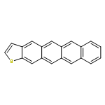

![Anthra[2,3-b:7,6-b']dithiophene](http://img.cochemist.com/ccimg/144500/144413-59-2.png)
![Anthra[2,3-b:7,6-b']dithiophene](http://img.cochemist.com/ccimg/144500/144413-59-2_b.png)
![Dinaphtho[2,3-b:2',3'-f]thieno[3,2-b]thiophene](/data/chemimg/136100/935280-42-5.png)
![Dinaphtho[2,3-b:2',3'-f]thieno[3,2-b]thiophene](/data/chemimg/136100/935280-42-5_b.png)
![Anthra[2,3-b:6,7-b']dithiophene](http://img.cochemist.com/ccimg/144500/144413-58-1.png)
![Anthra[2,3-b:6,7-b']dithiophene](http://img.cochemist.com/ccimg/144500/144413-58-1_b.png)