Co-reporter:Huanli Dong, Hongxiang Li, Erjing Wang, Zhongming Wei, Wei Xu, Wenping Hu and Shouke Yan
Langmuir December 2, 2008 Volume 24(Issue 23) pp:13241-13244
Publication Date(Web):November 6, 2008
DOI:10.1021/la8026094
Molecules of a rigid rod conjugated polymer, a derivative of poly(para-phenylene ethynylene)s with thioacetyl end groups (TA-PPE), were well aligned by drop-casting the polymer solution onto the friction-transferred poly(tetrafluoroethylene) substrates. TA-PPE molecules were found to be exactly oriented with their conjugated backbones along the PTFE sliding direction. Photoresponse characteristics based on the uniaxially ordered film were significantly improved compared to those of devices with the disordered film. For example, the switch on/off ratio of the photoswitchers with aligned molecules was as high as 330−400, while that of devices without alignment was only 8−12. It was due to the efficient carrier transport along the highly aligned polymer films, in which the molecules of TA-PPE oriented along the carrier transport direction of the devices.
Co-reporter:Yanqiu Sun;Dr. Yilong Lei; Liangsheng Liao; Wenping Hu
Angewandte Chemie International Edition 2017 Volume 56(Issue 35) pp:10352-10356
Publication Date(Web):2017/08/21
DOI:10.1002/anie.201702084
AbstractTwo typical types of luminescent organic cocrystals comprising pyrene–octafluoronaphthalene (pyrene–OFN) and pyrene–1,2,4,5-tetracyanobezene (pyrene–TCNB) were developed by a simple supramolecular assembly strategy. The cocrystals exhibit distinct optical properties because of their different intermolecular interaction modes; that is, arene–perfluoroarene (AP) and charge-transfer (CT) interactions. Unexpectedly, a pyrene–TCNB system with strong CT interactions was incorporated into a pyrene–OFN host as a robust guest to generate white-light emission (WLE). In the supramolecular cocrystal system, an efficient energy-transfer process from pyrene–OFN to pyrene–TCNB occurred because of the well-matched spectra of the constituents and a desirable energy donor/acceptor (D/A) distance. The present competitive intermolecular interaction strategy could be applied to the fabrication of more complicated organic light-harvesting systems.
Co-reporter:Yanqiu Sun;Dr. Yilong Lei; Liangsheng Liao; Wenping Hu
Angewandte Chemie International Edition 2017 Volume 56(Issue 35) pp:10249-10249
Publication Date(Web):2017/08/21
DOI:10.1002/anie.201706512
Pass with flying colors Efficient energy transfer from a charge-transfer host to an arene–perfluoroarene dopant generates stable white-light-emitting crystals. In their Communication on page 10352 ff., W. P. Hu et al. describe competing intermolecular charge-transfer and arene–perfluoroarene interactions in blue-light-emitting pyrene–octafluoronaphthalene cocrystals doped with an orange-light-emitting pyrene–1,2,4,5-tetracyanobenzene complex.
Co-reporter:Xiaoshuang Chen;Yunfeng Qiu;Guangbo Liu;Wei Zheng;Wei Feng;Feng Gao;Wenwu Cao;YongQing Fu;PingAn Hu
Journal of Materials Chemistry A 2017 vol. 5(Issue 22) pp:11357-11363
Publication Date(Web):2017/06/06
DOI:10.1039/C7TA02327H
This study presents the successful growth of defective 2D terrace MoSe2/CoMoSe lateral heterostructures (LH), bilayer and multilayer MoSe2/CoMoSe LH, and vertical heterostructures (VH) nanolayers by doping metal cobalt (Co) element into MoSe2 atomic layers to form a CoMoSe alloy at high temperatures (∼900 °C). After the successful introduction of metal Co heterogeneity in the MoSe2 thin layers, more active sites can be created to enhance hydrogen evolution reaction (HER) activities combining with metal Co catalysis through mechanisms such as (1) atomic arrangement distortion in CoMoSe alloy nanolayers, (2) atomic level coarsening in LH interfaces and terrace edge layer architecture in VH, and (3) formation of defective 2D terrace MoSe2 nanolayers heterogeneous catalyst via metal Co doping. The HER investigations indicated that the obtained products with LH and VH exhibited an improved HER activity in comparison with those from pristine 2D MoSe2 electrocatalyst and LH type MoSe2/CoMoSe. The present work shows a facile yet reliable route to introduce metal ions into ultrathin 2D transition metal dichalcogenides (TMDCS) and produce defective 2D alloy atomic layers for exposing active sites, eventually improving their electrocatalytic performance.
Co-reporter:Xiaoshuang Chen, Yunfeng Qiu, Huihui Yang, Guangbo Liu, Wei Zheng, Wei Feng, Wenwu Cao, Wenping Hu, and PingAn Hu
ACS Applied Materials & Interfaces 2017 Volume 9(Issue 2) pp:
Publication Date(Web):December 23, 2016
DOI:10.1021/acsami.6b13379
Considering the unique layered structure and novel optoelectronic properties of individual MoS2 and MoSe2, as well as the quantum coherence or donor–acceptor coupling effects between these two components, rational design and artificial growth of in-plane mosaic MoS2/MoSe2 lateral heterojunctions film on conventional amorphous SiO2/Si substrate are in high demand. In this article, large-area, uniform, high-quality mosaic MoS2/MoSe2 lateral heterojunctions film was successfully grown on SiO2/Si substrate for the first time by chemical vapor deposition (CVD) technique. MoSe2 film was grown along MoS2 triangle edges and occupied the blanks of the substrate, finally leading to the formation of mosaic MoS2/MoSe2 lateral heterojunctions film. The composition and microstructure of mosaic MoS2/MoSe2 lateral heterojunctions film were characterized by various analytic techniques. Photodetectors based on mosaic MoS2/MoSe2 lateral heterojunctions film, triangular MoS2 monolayer, and multilayer MoSe2 film are systematically investigated. The mosaic MoS2/MoSe2 lateral heterojunctions film photodetector exhibited optimal photoresponse performance, giving rise to responsivity, detectivity, and external quantum efficiency (EQE) up to 1.3 A W–1, 2.6 × 10¹¹ Jones, and 263.1%, respectively, under the bias voltage of 5 V with 0.29 mW cm–2 (610 nm), possibly due to the matched band alignment of MoS2 and MoSe2 and strong donor–acceptor delocalization effect between them. Taking into account the similar edge conditions of transition metal dichalcogenides (TMDCs), such a facile and reliable approach might open up a unique route for preparing other 2D mosaic lateral heterojunctions films in a manipulative manner. Furthermore, the mosaic lateral heterojunctions film like MoS2/MoSe2 in the present work will be a promising candidate for optoelectronic fields.Keywords: 2D material; lateral heterostructure; MoS2/MoSe2; mosaic; photodetector;
Co-reporter:Ke Zhou;Hongfeng Chen;Huanli Dong;Qi Fang
Science China Chemistry 2017 Volume 60( Issue 4) pp:510-515
Publication Date(Web):2017 April
DOI:10.1007/s11426-016-9011-9
Compact molecular packing with short π-π stacking and large π-overlap in organic semiconductors is desirable for efficient charge transport and high carrier mobility. Thus charge transport anisotropy along different directions is commonly observed in organic semiconductors. Interestingly, in this article, we found that comparable charge transport property were achieved based on the single crystals of a bis-fused tetrathiafulvalene derivative (EM-TTP) compound along two interaction directions, that is, the multiple strong S···S intermolecular interactions and the π-π stacking direction, with the measured electrical conductivity and hole mobility of 0.4 S cm−1, 0.94 cm2 V−1 s−1 and 0.2 S cm−1, 0.65 cm2 V−1 s−1, respectively. This finding provides us a new molecular design concept for developing novel organic semiconductors with isotropic charge transport property through the synergistic effect of multiple intermolecular interactions (such as S···S interactions) and π-π stacking.
Co-reporter:Zunzhi Wang;Rongjin Li;Yulan Chen;Yuan-Zhi Tan;Zeyi Tu;Xuejiao J. Gao;Huanli Dong;Yuanping Yi;Yu Zhang;Klaus Müllen;Long Chen
Journal of Materials Chemistry C 2017 vol. 5(Issue 6) pp:1308-1312
Publication Date(Web):2017/02/09
DOI:10.1039/C6TC04365H
We report a facile synthesis of novel angularly fused bistetracene derivatives where two tetracene skeletons are cata-annulated at three benzene rings. Compared with previously described examples, our bistetracenes exhibit a narrower HOMO–LUMO gap but still exhibit high stability. Attempted synthesis of di-substituted bistetracene (BT-2TIPS) also led to unexpected triple (BT-3TIPS) and four-fold (BT-4TIPS) alkylsilylethynyl substitution. The photophysical, electrochemical and optical properties as well as the solid-state structure of these three bistetracene analogues are investigated. A charge carrier mobility up to 0.42 cm2 V−1 s−1 was determined based on field effect transistors.
Co-reporter:Hanlin Wang;Hongtao Liu;Qiang Zhao;Zhenjie Ni;Ye Zou;Jie Yang;Lifeng Wang;Yanqiu Sun;Yunlong Guo;Yunqi Liu
Advanced Materials 2017 Volume 29(Issue 32) pp:
Publication Date(Web):2017/08/01
DOI:10.1002/adma.201701772
Human eyes use retina photoreceptor cells to absorb and distinguish photons from different wavelengths to construct an image. Mimicry of such a process and extension of its spectral response into the near-infrared (NIR) is indispensable for night surveillance, retinal prosthetics, and medical imaging applications. Currently, NIR organic photosensors demand optical filters to reduce visible interference, thus making filter-free and anti-visible NIR imaging a challenging task. To solve this limitation, a filter-free and conformal, retina-inspired NIR organic photosensor is presented. Featuring an integration of photosensing and floating-gate memory modules, the device possesses an acute color distinguishing capability. In general, the retina-like photosensor transduces NIR (850 nm) into nonvolatile memory and acts as a dynamic photoswitch under green light (550 nm). In doing this, a filter-free but color-distinguishing photosensor is demonstrated that selectively converts NIR optical signals into nonvolatile memory.
Co-reporter:Yanqiu Sun;Dr. Yilong Lei; Liangsheng Liao; Wenping Hu
Angewandte Chemie 2017 Volume 129(Issue 35) pp:10488-10492
Publication Date(Web):2017/08/21
DOI:10.1002/ange.201702084
AbstractTwo typical types of luminescent organic cocrystals comprising pyrene–octafluoronaphthalene (pyrene–OFN) and pyrene–1,2,4,5-tetracyanobezene (pyrene–TCNB) were developed by a simple supramolecular assembly strategy. The cocrystals exhibit distinct optical properties because of their different intermolecular interaction modes; that is, arene–perfluoroarene (AP) and charge-transfer (CT) interactions. Unexpectedly, a pyrene–TCNB system with strong CT interactions was incorporated into a pyrene–OFN host as a robust guest to generate white-light emission (WLE). In the supramolecular cocrystal system, an efficient energy-transfer process from pyrene–OFN to pyrene–TCNB occurred because of the well-matched spectra of the constituents and a desirable energy donor/acceptor (D/A) distance. The present competitive intermolecular interaction strategy could be applied to the fabrication of more complicated organic light-harvesting systems.
Co-reporter:Yanqiu Sun;Dr. Yilong Lei; Liangsheng Liao; Wenping Hu
Angewandte Chemie 2017 Volume 129(Issue 35) pp:10383-10383
Publication Date(Web):2017/08/21
DOI:10.1002/ange.201706512
Effizienter Energietransfer von einem Ladungstransfer-Wirt zu einem Aren-Perfluoraren-Dotanden führt zu Kristallen, die eine stabile weiße Strahlung abgeben. W. P. Hu et al. beschreiben in der Zuschrift auf S. 10488 konkurrierende intermolekulare Ladungstransfer- und Aren-Perfluoraren-Wechselwirkungen in blaues Licht emittierenden Pyren-Octafluornaphthalin-Cokristallen, die mit einem orangefarbenes Licht emittierenden Pyren-1,2,4,5-Tetracyanbenzol-Komplex dotiert sind.
Co-reporter:Weigang Zhu;Lingyun Zhu;Ye Zou;Yishi Wu;Yonggang Zhen;Huanli Dong;Hongbing Fu;Zhixiang Wei;Qiang Shi
Advanced Materials 2016 Volume 28( Issue 28) pp:5954-5962
Publication Date(Web):
DOI:10.1002/adma.201600280
Co-reporter:Hanlin Wang;Hongtao Liu;Qiang Zhao;Cheng Cheng;Yunqi Liu
Advanced Materials 2016 Volume 28( Issue 4) pp:624-630
Publication Date(Web):
DOI:10.1002/adma.201503953
Co-reporter:Zongrui Wang, Xiangguang Li, Ye Zou, Jiahui Tan, Xiaolong Fu, Jie Liu, Chengyi Xiao, Huanli Dong, Wei Jiang, Feng Liu, Yonggang Zhen, Zhaohui Wang, Thomas P. Russell and Wenping Hu
Journal of Materials Chemistry A 2016 vol. 4(Issue 30) pp:7230-7240
Publication Date(Web):23 Jun 2016
DOI:10.1039/C6TC01769J
A series of acceptor–donor–acceptor (A–D–A) conjugated molecules based on naphthalene diimide dimers bridged with different π-conjugated heterocyclic units (NDI–π–NDI) have been designed and synthesized. By an ingenious design strategy, the LUMO (the lowest unoccupied molecular orbital) of the NDI-based small molecules is well controlled to a relatively constant value of −3.8 to −3.9 eV, whereas their HOMO (the highest occupied molecular orbital) could be tuned over a wide range, from −6.5 eV (compound 1) to −5.5 eV (compound 5), leading to varied band gaps from 2.6 eV to 1.5 eV. Organic field-effect transistor (OFET) characterization of these NDI–π–NDI molecules shows that compounds 1, 2, and 3 have good n-type semiconducting properties in a N2 atmosphere with the maximum electron mobilities up to 0.15 cm2 V−1 s−1, 0.46 cm2 V−1 s−1 and 0.57 cm2 V−1 s−1, respectively. Compounds 4 and 5, due to the high-lying HOMO levels and reduced energy band gaps, have ambipolar semiconducting properties and OFETs based on 5 show the highest electron and hole mobilities up to 1.23 cm2 V−1 s−1 and 0.0074 cm2 V−1 s−1, respectively. Moreover, the performances are enhanced under thermal treatment because of the increased crystallinity as evidenced by X-ray diffraction (XRD) and atomic force microscopy (AFM). The easily tunable electronic energy levels make the NDI-based semiconductors promising n-channel and ambipolar components in organic devices.
Co-reporter:Shujun Yu, Xiangxue Wang, Yuejie Ai, Xiaoli Tan, Tasawar Hayat, Wenping Hu and Xiangke Wang
Journal of Materials Chemistry A 2016 vol. 4(Issue 15) pp:5654-5662
Publication Date(Web):11 Mar 2016
DOI:10.1039/C6TA00890A
The individual and competitive adsorption studies of benzene, aniline and naphthylamine on reduced graphene oxides (rGOs) were investigated by batch experiments and theoretical density functional theory (DFT). Experimental results indicate that (1) in all the single, binary, and ternary aromatic compound systems, the sequence of maximum adsorption capacity is naphthylamine > aniline > benzene on rGOs; (2) the overall adsorption capacity of rGOs is in the order of ternary > binary > single system. The DFT calculations indicate that (1) the adsorption energy (Ead) follows the order of Ead (benzene) < Ead (aniline) < Ead (naphthylamine); (2) the binding energy (Ebd) values of aromatic mixtures indicate that the intra-molecular interactions between the aromatic compounds themselves have an important influence on their adsorption on rGOs. The DFT calculations are in good agreement with the batch adsorption results. These findings are very important and useful to understand the mechanisms of adsorption of aromatic compounds on rGOs as well as assessing the effect of the benzene-ring number and polar functional groups on the adsorption of coexisting aromatic compounds on rGOs. The contents are important for the application of rGOs in environmental pollution management.
Co-reporter:Jie Liu, Weigang Zhu, Ke Zhou, Zongrui Wang, Ye Zou, Qing Meng, Jie Li, Yonggang Zhen and Wenping Hu
Journal of Materials Chemistry A 2016 vol. 4(Issue 16) pp:3621-3627
Publication Date(Web):24 Mar 2016
DOI:10.1039/C6TC00499G
We report here a systematic study of the solid-state packing, optoelectronic properties and organic field-effect transistor properties of three isomeric 2,6-di-pyridyl anthracene derivatives (1a, 1b and 1c). Very different solid-state physicochemical behaviours were found as a result of the subtle change in the substitution site, especially in the solid-state emission and charge transport properties. For 1a and 1b, which adopted H-like aggregates in the solid state, a bright blue emission with fluorescent quantum efficiencies (ΦF) of 50.2 and 17.5% and thin film mobilities of 0.05 and 10−5 cm2 V−1 s−1, respectively, were obtained. The inferior mobility of 1b might be caused by the larger torsion and herringbone angle in the solid-state packing. A green emission with ΦF of 16% was obtained for single crystals of 1c. No charge transport property was observed for 1c, which might be related to the unfavourable solid-state packing and poor film morphology.
Co-reporter:Zongrui Wang, Huanli Dong, Ye Zou, Qiang Zhao, Jiahui Tan, Jie Liu, Xiuqiang Lu, Jinchong Xiao, Qichun Zhang, and Wenping Hu
ACS Applied Materials & Interfaces 2016 Volume 8(Issue 12) pp:7919
Publication Date(Web):March 11, 2016
DOI:10.1021/acsami.5b12307
Poor charge injection and transport at the electrode/semiconductor contacts has been so far a severe performance hurdle for bottom-contact bottom-gate (BCBG) organic field-effect transistors (OFETs). Here, we have developed a simple, economic, and effective method to improve the carrier injection efficiency and obtained high-performance devices with low cost and widely used source/drain (S/D) electrodes (Ag/Cu). Through the simple electrode etching process, the work function of the electrodes is more aligned with the semiconductors, which reduces the energy barrier and facilitates the charge injection. Besides, the formation of the thinned electrode edge with desirable micro/nanostructures not only leads to the enlarged contact side area beneficial for the carrier injection but also is in favor of the molecular self-organization for continuous crystal growth at the contact/active channel interface, which is better for the charge injection and transport. These effects give rise to the great reduction of contact resistance and the amazing improvement of the low-cost bottom-contact configuration OFETs performance.Keywords: bottom-contact organic field-effect transistor; contact resistance; low-cost electrode; micro/nanostructures; soft-etching method
Co-reporter:Yong-Gang Zhen, Huan-Li Dong, Lang Jiang, Wen-Ping Hu
Chinese Chemical Letters 2016 Volume 27(Issue 8) pp:1330-1338
Publication Date(Web):August 2016
DOI:10.1016/j.cclet.2016.06.023
As a quite ubiquitous phenomenon, crystal polymorph is one of the key issues in the field of organic semiconductors. This review gives a brief summary to the advances on polymorph control of thin film and single crystal of representative organic semiconductors towards high-performance field-effect transistors. Particularly, the relationship between crystal polymporh and charge transport behaviour has been discussed to shed light on the rational preparation of outstanding organic semiconducting materials with desired crystal polymorph.The advances on polymorph control of representative organic semiconductors towards high-performance field-effect transistors are briefly discussed.Download high-res image (130KB)Download full-size image
Co-reporter:Xi Zhang, Suna Zhang, Liqiang Li, Xiaosong Chen, Zeyang Xu, Kunjie Wu, Hongwei Li, Yancheng Meng, Wenchong Wang, Wenping Hu, Lifeng Chi
Solid-State Electronics 2016 Volume 123() pp:51-57
Publication Date(Web):September 2016
DOI:10.1016/j.sse.2016.05.020
•A bottom-up in-situ polymerization strategy is utilized to produce the surface-grafting PPY electrodes.•The patterned PPY electrodes may serve as good electrode to efficiently drive organic complementary inverters.•The inverter with PPY electrodes exhibits an operation frequency of several kHz.Surface-grafting conducting polymer has advantage to circumvent the difficulty in patterning as well as the weak interface adhesion on substrate of the conventional conducting polymer, which would be desirable for its application as electrodes in electronic devices. In this work, the patterned surface-grafting polypyrrole (PPY) is used as electrode, which shows merits such as strong interface adhesion, robustness against solvent treatment, easy scaling-up, and good conductivity. Remarkably, the surface-grafting PPY electrodes can efficiently drive both p-type and n-type organic field-effect transistors. By combining p-/n-type transistors, organic complementary inverters are constructed with PPY electrodes, which exhibit low operational voltage (<8 V), high gain (6–17), and low power dissipation (several tens of nW). The switching voltage is approximately 0.5Vdd with a high noise margin (>70% of 0.5Vdd). Dynamic switching measurements indicate that the inverter has an operational frequency of about 3.3 kHz. This is the first report on kilohertz organic complementary inverter driven with surface-grafting conducting polymer electrodes. High device performance, together with the facile patternability and other merits, may promote the application of surface-grafting conducting polymer electrode in the field of organic electronics.Organic complementary inverters driven by surface-grafting conducting polypyrrole electrodes are demonstrated. The inverters show a high operation frequency of about 3.3 kHz, low operational voltage (<8 V), high gain (6–17), low power dissipation (several tens of nW), and large noise margin (>70% ½ Vdd). This work may promote the application of surface-grafting conducting polymer electrode in organic electronics.
Co-reporter:Wenping Hu
Science China Materials 2016 Volume 59( Issue 6) pp:410-411
Publication Date(Web):2016 June
DOI:10.1007/s40843-016-5045-x
Co-reporter:Chunhui Xu;Dr. Ping He;Dr. Jie Liu;Dr. Ajuan Cui;Dr. Huanli Dong;Dr. Yonggang Zhen; Wei Chen; Wenping Hu
Angewandte Chemie 2016 Volume 128( Issue 33) pp:9671-9675
Publication Date(Web):
DOI:10.1002/ange.201602781
Abstract
Two-dimensional (2D) crystals of organic semiconductors (2DCOS) have attracted attention for large-area and low-cost flexible optoelectronics. However, growing large 2DCOS in controllable ways and transferring them onto technologically important substrates, remain key challenges. Herein we report a facile, general, and effective method to grow 2DCOS up to centimeter size which can be transferred to any substrate efficiently. The method named “solution epitaxy” involves two steps. The first is to self-assemble micrometer-sized 2DCOS on water surface. The second is epitaxial growth of them into millimeter or centimeter sized 2DCOS with thickness of several molecular layers. The general applicability of this method for the growth of 2DCOS is demonstrated by nine organic semiconductors with different molecular structures. Organic field-effect transistors (OFETs) based on the 2DCOS demonstrated high performance, confirming the high quality of the 2DCOS.
Co-reporter:Chunhui Xu;Dr. Ping He;Dr. Jie Liu;Dr. Ajuan Cui;Dr. Huanli Dong;Dr. Yonggang Zhen; Wei Chen; Wenping Hu
Angewandte Chemie 2016 Volume 128( Issue 33) pp:
Publication Date(Web):
DOI:10.1002/ange.201605080
Co-reporter:Chunhui Xu;Dr. Ping He;Dr. Jie Liu;Dr. Ajuan Cui;Dr. Huanli Dong;Dr. Yonggang Zhen; Wei Chen; Wenping Hu
Angewandte Chemie International Edition 2016 Volume 55( Issue 33) pp:
Publication Date(Web):
DOI:10.1002/anie.201605080
Co-reporter:Xi Zhang;Xiaosong Chen;Jie Liu;Yonggang Zhen;Huanli Dong
Science China Chemistry 2016 Volume 59( Issue 12) pp:1645-1650
Publication Date(Web):2016 December
DOI:10.1007/s11426-016-0098-y
The physical and chemical properties of organic semiconductors are closely related to their aggregation structure. Tuning of aggregation structure and electrical property is important for the application in organic electronics. In this study, a facile way to tune the aggregation structure and electrical property of 2.6-diphenyl-anthracene (DPA) is realized by using the octadecyltrichlorosilane (OTS) modification layer with different density which is fabricated by controlling reaction temperature and time. Compared with low density OTS, DPA forms larger grain size, less grain boundaries, and better molecular ordering on high density OTS surface. As a result, the charge transporting mobility of DPA film on high density OTS surface is about two orders of magnitude higher than that on low density OTS surface. The tunable aggregation structure and electrical property of DPA demonstrated here would be meaningful for the application of DPA in organic electronics.
Co-reporter:Hantang Zhang;Lang Jiang;Yonggang Zhen;Jing Zhang;Guangchao Han;Xiaotao Zhang;Xiaolong Fu;Yuanping Yi;Wei Xu;Huanli Dong;Wei Chen;Daoben Zhu
Advanced Electronic Materials 2016 Volume 2( Issue 6) pp:
Publication Date(Web):
DOI:10.1002/aelm.201500423
Co-reporter:Chunhui Xu;Dr. Ping He;Dr. Jie Liu;Dr. Ajuan Cui;Dr. Huanli Dong;Dr. Yonggang Zhen; Wei Chen; Wenping Hu
Angewandte Chemie International Edition 2016 Volume 55( Issue 33) pp:9519-9523
Publication Date(Web):
DOI:10.1002/anie.201602781
Abstract
Two-dimensional (2D) crystals of organic semiconductors (2DCOS) have attracted attention for large-area and low-cost flexible optoelectronics. However, growing large 2DCOS in controllable ways and transferring them onto technologically important substrates, remain key challenges. Herein we report a facile, general, and effective method to grow 2DCOS up to centimeter size which can be transferred to any substrate efficiently. The method named “solution epitaxy” involves two steps. The first is to self-assemble micrometer-sized 2DCOS on water surface. The second is epitaxial growth of them into millimeter or centimeter sized 2DCOS with thickness of several molecular layers. The general applicability of this method for the growth of 2DCOS is demonstrated by nine organic semiconductors with different molecular structures. Organic field-effect transistors (OFETs) based on the 2DCOS demonstrated high performance, confirming the high quality of the 2DCOS.
Co-reporter:Guangyao Zhao;Pengcheng Gu;Huanli Dong;Wei Jiang;Zhaohui Wang
Advanced Electronic Materials 2016 Volume 2( Issue 5) pp:
Publication Date(Web):
DOI:10.1002/aelm.201500430
Co-reporter:Chengyi Xiao;Guangyao Zhao;Andong Zhang;Wei Jiang;René A. J. Janssen;Weiwei Li;Zhaohui Wang
Advanced Materials 2015 Volume 27( Issue 34) pp:4963-4968
Publication Date(Web):
DOI:10.1002/adma.201502617
Co-reporter:Congcong Zhang;Penglei Chen;Huanli Dong;Yonggang Zhen;Minghua Liu
Advanced Materials 2015 Volume 27( Issue 36) pp:5379-5387
Publication Date(Web):
DOI:10.1002/adma.201501273
One-dimensional (1D) solid-state supramolecular structures based on porphyrin chromophores arouse numerous expectations from the interdisciplinary scientific communities of supramolecular chemistry and advanced soft materials science. This stems from the intrinsic assembly capability of porphyrins to form various well-defined 1D assemblies, which have broad opportunities in the fields of advanced soft matter. A brief review on 1D porphyrin micro-/nanoassemblies constructed via surfactant-assisted self-assembly is presented here, in terms of addressing new ideas recently developed for controlled assembly, hierarchical organization, and new-type functional surfactants etc. The functionalization of the as-assembled 1D structures with regard to supramolecular photocatalysis, non-linear optics, nanoelectronic gas sensors, photoelectrochemical solar cells, etc. is highlighted.
Co-reporter:Ajuan Cui;Zhe Liu;Huanli Dong;Yujin Wang;Yonggang Zhen;Wuxia Li;Junjie Li;Changzhi Gu
Advanced Materials 2015 Volume 27( Issue 19) pp:3002-3006
Publication Date(Web):
DOI:10.1002/adma.201500527
Co-reporter:Ping He;Zeyi Tu;Guangyao Zhao;Yonggang Zhen;Hua Geng;Yuanping Yi;Zongrui Wang;Hantang Zhang;Chunhui Xu;Jie Liu;Xiuqiang Lu;Xiaolong Fu;Qiang Zhao;Xiaotao Zhang;Deyang Ji;Lang Jiang;Huanli Dong
Advanced Materials 2015 Volume 27( Issue 5) pp:825-830
Publication Date(Web):
DOI:10.1002/adma.201404806
Co-reporter:Jie Liu, Lingqiang Meng, Weigang Zhu, Congcong Zhang, Hantang Zhang, Yifan Yao, Zongrui Wang, Ping He, Xiaotao Zhang, Ying Wang, Yonggang Zhen, Huanli Dong, Yuanping Yi and Wenping Hu
Journal of Materials Chemistry A 2015 vol. 3(Issue 13) pp:3068-3071
Publication Date(Web):05 Feb 2015
DOI:10.1039/C4TC02964J
Cross-dipole stacking has been addressed as a preferred motif for solid state emission, but inefficient for charge transport. Here we synthesize a new anthracene derivative, which adopts cross-stacking in the solid state with a solid state fluorescence up to 77.3% and a hole mobility of 1.47 cm2 V−1 s−1, integrating optical and electrical properties successfully. As far as we know, it is the first report of organic field-effect transistors based on cross-dipole stacking molecules.
Co-reporter:Guorui Wang, Qingxin Tang, Yanhong Tong, Wenping Hu and Yichun Liu
Journal of Materials Chemistry A 2015 vol. 3(Issue 37) pp:9749-9749
Publication Date(Web):02 Sep 2015
DOI:10.1039/C5TC90164B
Correction for ‘Individual single-crystal nanowires as electrodes for organic single-crystal nanodevices’ by Guorui Wang et al., J. Mater. Chem. C, 2015, DOI: 10.1039/c5tc01920f.
Co-reporter:Jie Li, Jie Liu, Yonggang Zhen, Lingqiang Meng, Ying Wang, Huanli Dong and Wenping Hu
Journal of Materials Chemistry A 2015 vol. 3(Issue 41) pp:10695-10698
Publication Date(Web):21 Sep 2015
DOI:10.1039/C5TC02254A
By simply introducing the naphthyl group into the 2-position of anthracene, we synthesized a new anthracene derivative, NaAnt, which showed good charge transporting properties up to 1.10 cm2 V−1 s−1 and a photoluminescence quantum yield (PLQY) of 40.30%. The results indicate its potential applications in multifunctional optoelectronics.
Co-reporter:Chong Kang, Jicheng Zhang, Huanli Dong, Wenping Hu and Zhishan Bo
Journal of Materials Chemistry A 2015 vol. 3(Issue 46) pp:12083-12089
Publication Date(Web):30 Oct 2015
DOI:10.1039/C5TC02369F
Four planar conjugated polymers called CZ-BO8, CZ-BO12, CZ-BT8 and CZ-BT12 with carbazole as the donor unit and benzooxadiazole or benzothiadiazole as the acceptor unit have been synthesized and characterized. These four polymers have medium band gaps (1.95–1.97 eV), low lying highest occupied molecular orbital energy levels (below −5.5 eV), relatively high hole mobilities (in the range of 0.026–0.1 cm2 V−1 s−1), and on/off current ratio of 106 without any post-treatment. Furthermore, high performance thin film phototransistors based on these four polymers have also been fabricated with high photocurrent/dark current ratios (5.7 × 10³–8.2 × 10³). Interestingly, phototransistors based on CZ-BO8 and CZ-BO12 show a faster photoresponse than that based on CZ-BT8 and CZ-BT12, providing valuable molecular design guidelines for high performance photoresponse polymers.
Co-reporter:Guorui Wang, Qingxin Tang, Yanhong Tong, Wenping Hu and Yichun Liu
Journal of Materials Chemistry A 2015 vol. 3(Issue 37) pp:9534-9539
Publication Date(Web):05 Aug 2015
DOI:10.1039/C5TC01920F
Conductive, transparent, and flexible SnO2:Sb single-crystal nanowires are shown as electrodes for F16CuPc single-crystal nanowire devices on flexible plastic, which includes anisotropic-transport OFETs, electrode-movable OFETs, and p–n junction photovoltaic devices. The SnO2:Sb nanowires provide a good energy level match and excellent soft contact with F16CuPc nanowires, leading to multifaceted applications of the SnO2:Sb nanowire in nanowire electronics and optoelectronics, as well as high device performance. Combined with their good size compatibility, these results show that the conductive SnO2:Sb single-crystal nanowire opens a window into the fundamental understanding of the intrinsic properties of highly ordered organic semiconductors, optimization and miniaturization of organic nanocircuits, and development of new-generation flexible organic nanodevices.
Co-reporter:Xiaotao Zhang, Guangyao Zhao, Yonggang Zhen, Zeyi Tu, Ping He, Yuanping Yi, Huanli Dong and Wenping Hu
Journal of Materials Chemistry A 2015 vol. 3(Issue 21) pp:5368-5371
Publication Date(Web):27 Apr 2015
DOI:10.1039/C5TC00606F
Two oxidation-stable naphthalenyl ethynyl anthracene derivatives have been synthesized via Sonogashira coupling. In contrast to a 1-position substituted anthracene derivative with near zero mobility, the functionalization at the 2-position of anthracene gives rise to a densely packed structure and a uniform film with mobility up to 1.6 cm2 V−1 s−1, which is one of the highest values for thin film transistors based on anthracene derivatives.
Co-reporter:Yingfeng Wang, Sufen Zou, Jianhua Gao, Huarong Zhang, Guoqiao Lai, Chengdong Yang, Hui Xie, Renren Fang, Hongxiang Li and Wenping Hu
Chemical Communications 2015 vol. 51(Issue 60) pp:11961-11963
Publication Date(Web):22 May 2015
DOI:10.1039/C5CC03305E
A novel two-dimensional organic semiconductor material [1]benzothieno[3,2-b][1]benzothieno[2,1-b:3,4-b′:6,5-b′′:7,8-b′′′]tetra(benzothiophene) (BTBTTBT) which largely extends the scope of the π-conjugated framework of heteroarene through “H” configuration was synthesized and its thermal, optical and electrochemical properties were investigated. This 2D molecule enables the easy growth of single-crystalline microribbons by the physical vapor transport method, which were evidenced by XRD, SEM and TEM. The single-crystalline OFET devices were fabricated based on the individual BTBTTBT microribbon and the remarkable high mobility of 17.9 cm2 V−1 s−1 and on/off ratios of over 107 could be achieved.
Co-reporter:Jie Liu, Huanli Dong, Zongrui Wang, Deyang Ji, Changli Cheng, Hua Geng, Hantang Zhang, Yonggang Zhen, Lang Jiang, Hongbing Fu, Zhishan Bo, Wei Chen, Zhigang Shuai and Wenping Hu
Chemical Communications 2015 vol. 51(Issue 59) pp:11777-11779
Publication Date(Web):09 Jun 2015
DOI:10.1039/C4CC10348C
An anthracene derivative, 2,6-diphenyl anthracene (DPA), was successfully synthesized with three simple steps and a high yield. The compound was determined to be a durable high performing semiconductor with thin film device mobility over 10 cm2 V−1 s−1. The efficient synthesis and high performance indicates its great potential in organic electronics.
Co-reporter:Ran Du;Zhe Zheng;Nannan Mao;Na Zhang;Jin Zhang
Advanced Science 2015 Volume 2( Issue 1-2) pp:
Publication Date(Web):
DOI:10.1002/advs.201400006
Co-reporter:Xiaotao Zhang, Chengyi Xiao, Andong Zhang, Fangxu Yang, Huanli Dong, Zhaohui Wang, Xiaowei Zhan, Weiwei Li and Wenping Hu
Polymer Chemistry 2015 vol. 6(Issue 26) pp:4775-4783
Publication Date(Web):22 May 2015
DOI:10.1039/C5PY00538H
Five wide or medium band gap diketopyrrolopyrrole (DPP)-based conjugated polymers with pyridine as bridges were developed for organic field-effect transistors (OFETs) and polymer solar cells (PSCs). By introducing copolymerized aromatic building blocks from strong electron-donating units to electron-deficient units into the conjugated backbone, the highest occupied molecular orbital (HOMO) and lowest unoccupied molecular orbital (LUMO) levels of the DPP polymers were tailored to the low-lying position. Therefore, the polarity of charge transport in OFETs can be switched from p-type to n-type. The DPP polymer with a low-lying LUMO of −3.80 eV provides a hole-only mobility of 2.95 × 10⁻² cm2 V−1 s−1, while an electron-only mobility of 1.24 × 10⁻³ cm2 V−1 s−1 is found in the DPP polymer with a LUMO of −4.22 eV. Further investigation of photovoltaic cells based on these DPP polymers shows a modest power conversion efficiency (PCE) of around 2%. Our results demonstrate that wide band gap pyridine-bridged DPP polymers have potential application in OFETs and OSCs by adjusting their energy level with alternated units on the conjugated backbone.
Co-reporter:Liangfu He, Zhuoyu Ji, Yonggang Zhen, Jie Liu, Fangxu Yang, Qiang Zhao, Huanli Dong and Wenping Hu
Physical Chemistry Chemical Physics 2015 vol. 17(Issue 40) pp:26541-26544
Publication Date(Web):30 Jan 2015
DOI:10.1039/C4CP06064D
Using single-displacement controlled spontaneous electrolysis solution-prepared CuTCNQ microribbons as the source/drain electrodes, we have fabricated 9,10-bis(2-phenylethynyl)anthracene (BEPA) based organic single crystal top-contact field-effect transistors. The interfacial energetic match between organic semiconductors and CuTCNQ electrodes with the low contact resistance accounts for the compelling improvement in electrical characteristics relative to the copper electrode, even comparable to gold counterparts. Furthermore, we have estimated the contact resistance of single-crystal transistors by the transfer line method (TLM).
Co-reporter:Zongrui Wang, Jianfeng Zhao, Huanli Dong, Ge Qiu, Qichun Zhang and Wenping Hu
Physical Chemistry Chemical Physics 2015 vol. 17(Issue 40) pp:26519-26524
Publication Date(Web):20 May 2015
DOI:10.1039/C5CP01302J
A new naphthalene diimide (NDI) derivative with an asymmetric aromatic backbone of 2-tetradecylbenzo[lmn]benzo[4,5]imidazo[2,1-b][3,8]phenanthroline-1,3,6(2H)-trione (IZ0) was designed and synthesized. Low LUMO level, large energy gap, and high thermal stability are characterized for this IZ0 compound. The OFET devices based on an IZ0 semiconductor exhibit typical n-type behavior. Through continuously optimizing the fabrication conditions, high performance n-channel OFETs were fabricated based on IZ0 films and single crystals, with the highest carrier mobility of 0.072 cm2 V−1 s−1 and 0.22 cm2 V−1 s−1, respectively.
Co-reporter:Yingfeng Wang, Sufen Zou, Jianhua Gao, Haixia Zhang, Guoqiao Lai, Hui Xie, Chengdong Yang, Hongxiang Li and Wenping Hu
RSC Advances 2015 vol. 5(Issue 39) pp:31018-31023
Publication Date(Web):26 Mar 2015
DOI:10.1039/C5RA03659C
A series of new naphthalene oligomers were designed and synthesized through linking at the α- and β-position of the terminal substituents. Optical and electrochemical measurements and DFT simulation revealed the distinctly different electronic structure of the α-position and β-position linked oligomers. The naphthalene oligomer linked at the α-position of benzothiophene exhibits excellent field-effect performances, with mobility as high as 0.13 cm2 V−1 s−1 and on/off ratio over 106. The significant difference of the OFET performances and thin film microstructures between the naphthalene oligomers also confirmed that the substituted position has an important effect on the properties of semiconductor materials and the α-position linked oligomer is better than β-position linked isomers.
Co-reporter:Xiangye Qi, Sufen Zou, Xiaoxia Liu, Wanglong Hao, Huarong Zhang, Zhanzhan Zang, Haixia Zhang, Jianhua Gao and Wenping Hu
New Journal of Chemistry 2015 vol. 39(Issue 2) pp:1045-1050
Publication Date(Web):18 Nov 2014
DOI:10.1039/C4NJ01590H
A novel benzoannulated pentathienoacene derivative dihexyl-[1]benzothieno[2′′,3′′:4′,5′]thieno[2′′,3′′:4,5;5′′,4′′:4′,5′]bisthieno[3,2-b:3′,2′-b′][1]benzothiophene was designed and synthesized. UV-vis spectra, electrochemistry and thermogravimetric analysis results reveal that this material has a large energy bandgap, low-lying highest occupied molecular orbital level and good thermal stability. Atomic force microscopy demonstrates that the thin films show high surface roughness and consisted of interconnected sheet-like crystalline grains. A highly ordered aggregation structure in grains was evidenced by X-ray diffraction measurements. Mobility up to 0.04 cm2 V−1 s−1 and an on/off ratio over 105 were achieved for the thin film field-effect transistors. These results suggest that this new benzoannulated pentathienoacene derivative is an important member of the thienoacene family and will contribute to a comprehensive analysis of the structure–property relationship of the thienoacene analogue.
Co-reporter:Chen Zhang, Guangyao Zhao, Weixuan Zeng, Kui Tian, Huanli Dong, Wenping Hu, Jingui Qin, Chuluo Yang
Organic Electronics 2015 Volume 16() pp:101-108
Publication Date(Web):January 2015
DOI:10.1016/j.orgel.2014.11.001
•A new copolymer of P(DTCBTZ) containing DTCDI and BTZ has been synthesized.•The HOMO and LUMO of P(DTCBTZ) are suitable for ambipolar charge transport.•P(DTCBTZ) showed balanced hole and electron mobility.A new copolymer P(DTCBTZ) of dithienocoronenediimide (DTCDI) and benzo(bis)thiadiazole (BTZ) as the active layer of organic field-effect transistors (OFETs) is reported. The combination of DTCDI with long alkyl chains and BTZ without alkyl chains results in reduced steric hindrance between acceptors of different polymer backbones. 2,2′-bithiophene is introduced into P(DTCBTZ), and thus donor–acceptor (D–A) interactions are induced. Absorption spectra of solution and thin films of P(DTCBTZ) reveal the existence of relatively strong aggregations of P(DTCBTZ) copolymers in solid state. The new copolymer of P(DTCBTZ) has a HOMO of −5.54 eV and a LUMO of −3.72 eV, which are suitable for both hole and electron transport. Bottom-gate and top-contact (BGTC) transistors were prepared and balanced charge transport was observed, with hole mobility of 0.018 cm2 V−1 s−1 and electron mobility of 0.019 cm2 V−1 s−1, indicating potential for application of polymers containing DTCDI in ambipolar semiconductors.
Co-reporter:Yunze Li, Deyang Ji, Huanli Dong, Jingze Li and Wenping Hu
RSC Advances 2015 vol. 5(Issue 107) pp:88059-88062
Publication Date(Web):06 Oct 2015
DOI:10.1039/C5RA17382E
In this work, the properties of polyimide (PI) as a dielectric film are systematically investigated. PI films are processed using a spin-coating method under various conditions. Subsequently, the leakage current, unit-area capacitance and morphologies of these films are characterized. Then the anti-solvent property is certified upon comparing the films before and after solvent treatment. Organic field-effect transistors based on PI dielectric films and pentacene active films show uniform performance distribution over a large area. Furthermore, a single crystal of 2,7-dihexyl-dibenzo[d,d′]thieno[3,2-b;4,5-b′]dithiophene (C6-DBTDT) is obtained on the PI film using a solution-processed method and exhibits good electrical properties with the highest mobility of 3 cm2 V−1 s−1 and Ion/Ioff > 105. It is believed that this kind of PI polymer dielectric film has potential applications in solution-processed, flexible and large-area organic electronics.
Co-reporter:Liangfu He;Deyang Ji;Erjing Wang;Yonggang Zhen;Huanli Dong
Science China Chemistry 2015 Volume 58( Issue 6) pp:1027-1031
Publication Date(Web):2015 June
DOI:10.1007/s11426-014-5240-6
The organic single-crystal field-effect transistors using anthracene derivative, H-Ant as an active layer with source/drain electrodes decorated by metal charge transfer salt (CuTCNQ) were fabricated. We demonstrated that this bottom-contact structure displayed an obvious improvement in the electrical characteristics relative to their pristine copper and top-contact gold electrode counterparts. This observation could be ascribed to the lower contact resistance resulting from the energetic match between electrodes and semiconductor.
Co-reporter:Weigang Zhu;Dr. Renhui Zheng;Xiaolong Fu; Hongbing Fu; Qiang Shi;Dr. Yonggang Zhen;Dr. Huanli Dong; Wenping Hu
Angewandte Chemie International Edition 2015 Volume 54( Issue 23) pp:6785-6789
Publication Date(Web):
DOI:10.1002/anie.201501414
Abstract
A new crystal of a charge-transfer (CT) complex was prepared through supramolecular assembly and it has unique two-dimensional (2D) morphology. The CT nature of the ground and excited states of this new Bpe-TCNB cocrystal (BTC) were confirmed by electron spin resonance measurements, spectroscopic studies, and theoretical calculations, thus providing a comprehensive understanding of the CT interactions in organic donor–acceptor systems. And the lowest CT1 excitons are responsible for the efficient photoluminescence (ΦPL=19 %), which can actively propagate in individual 2D BTCs without anisotropy, thus implying that the optical waveguide property of the crystal is not related to the molecular stacking structure. This unique 2D CT cocrystal exhibits potential for use in functional photonic devices in the next-generation optoelectronic communications.
Co-reporter:Weigang Zhu;Dr. Renhui Zheng;Xiaolong Fu; Hongbing Fu; Qiang Shi;Dr. Yonggang Zhen;Dr. Huanli Dong; Wenping Hu
Angewandte Chemie 2015 Volume 127( Issue 23) pp:6889-6893
Publication Date(Web):
DOI:10.1002/ange.201501414
Abstract
A new crystal of a charge-transfer (CT) complex was prepared through supramolecular assembly and it has unique two-dimensional (2D) morphology. The CT nature of the ground and excited states of this new Bpe-TCNB cocrystal (BTC) were confirmed by electron spin resonance measurements, spectroscopic studies, and theoretical calculations, thus providing a comprehensive understanding of the CT interactions in organic donor–acceptor systems. And the lowest CT1 excitons are responsible for the efficient photoluminescence (ΦPL=19 %), which can actively propagate in individual 2D BTCs without anisotropy, thus implying that the optical waveguide property of the crystal is not related to the molecular stacking structure. This unique 2D CT cocrystal exhibits potential for use in functional photonic devices in the next-generation optoelectronic communications.
Co-reporter:Ajuan Cui;Zhe Liu;Huanli Dong;Yujin Wang;Yonggang Zhen
Science China Materials 2015 Volume 58( Issue 10) pp:769-774
Publication Date(Web):2015 October
DOI:10.1007/s40843-015-0092-8
Construction of molecular devices is one of the most promising approaches for the ultimate miniaturization of electronic devices, the groundwork of which is the fabrication of nanogap electrodes. Here we report a method to fabricate nanogap electrodes through thermal annealing based on single grain boundary junction. By performing low temperature thermal process, single grain boundary junction can be broken and change into a suspended gap with gap width down to sub-5 nanometers, which is beyond the fabrication precision of traditional lithography technologies. With the advantage of shape stability, no debris and high time efficiency, such nanogap electrodes is promising in constructing molecular devices with two or three-terminals.纳米尺度分子器件是最有可能实现超高密度集成电路的途径之一, 而纳米间隙电极对的制备是分子器件的构筑基础. 本文利用热处理诱导晶间断裂现象来进行纳米间隙电极对的构筑. 通过低温热处理过程实现单个金晶界结的断裂, 使其从晶界结转化为悬空纳米间隙电极对. 所制备的纳米间隙电极对的间隙尺寸可达到亚5纳米, 采用 传统的微纳米加工方法很难实现该尺寸间隙电极对. 利用热处理诱导晶间断裂所制备的纳米间隙电极对具有诸多优点, 如形状稳定性好、间隙中无杂质颗粒残留等, 有望用来构筑两端或三端分子器件.
Co-reporter:Guangyao Zhao;Jie Liu;Qing Meng;Deyang Ji;Xiaotao Zhang;Ye Zou;Yonggang Zhen;Huanli Dong
Advanced Electronic Materials 2015 Volume 1( Issue 8) pp:
Publication Date(Web):
DOI:10.1002/aelm.201500071
Obvious differentiated response of organic phototransistors (OPTs) to the lights with different wavelengths is a challenge but a prerequisite for wavelength-selective applications. In this manuscript, highly UV-sensitive OPTs are fabricated based on benzo[1,2-b:4,5-b′]dithiophene dimers (BBDT, BBDTE, and BBDTY). The BBDTE-based organic single-crystal transistors (OSCTs), which show carrier mobility up to 1.62 cm2 V−1 s−1, exhibit a maximum photoresponsivity up to 9821 A W−1 and a maximum photosensitivity up to 105 towards UV light (37 μW cm−2), and the photosensitivity observed within tested light intensity range is unexpectedly stable. The BBDTY-based OPTs also exhibit differentiated response between UV and visible lights, even with thin-film state of organic semiconductor, and the highest photoresponsivity and photosensitivity to UV light reached 9336 A W−1 and 4429, respectively. This selective and highly sensitive performance enables unsaturated bond-linked benzo[1,2-b:4,5-b′]dithiophene dimers promising candidates for UV detectors.
Co-reporter:Weigang Zhu;Huanli Dong;Yonggang Zhen
Science China Materials 2015 Volume 58( Issue 11) pp:854-859
Publication Date(Web):2015 November
DOI:10.1007/s40843-015-0099-1
Organic cocrystal (also “co-crystal”), formed with two or more different components via non-covalent intermolecular interactions, possesses novel, unpredicted and unique properties, which are not the simple sum of those molecular components, e.g., with effect of 1+1>2. In this regard, organic cocrystals provide a distinctive strategy for the synthesis of novel multifunctional materials, and an important platform for exploring new fundamental physicochemical phenomena in molecular systems, such as high conductivity, ambipolar charge transportation, photovoltaic behavior, white light-emitting, room-temperature phosphorescence, nonlinear optics and ferroelectricity etc., with potential application even in liquid crystal engineering and drug industry.本文简明扼要地介绍了“有机共晶”这个重要研究领域的兴起和发展过程, 在有争议的方面, 如共晶定义和如何判定分子排布等, 给出了作者独到的见解. 特别重要的是, 通过阐述该领域当前存在的问题和挑战, 结合分析最新的研究进展和结果, 使得人们对共晶的认识更为系统和深入. 基于此, 作者同时分析和指出了未来可能重点发展的研究方向.
Co-reporter:Xiang Qin;Huanli Dong
Science China Materials 2015 Volume 58( Issue 3) pp:186-191
Publication Date(Web):2015 March
DOI:10.1007/s40843-015-0035-4
Organic-inorganic halide perovskites have attracted considerable attention owing to their outstanding solar cell efficiency. Meanwhile, these halide perovskites exhibit good light emitting in visible and near-infrared range with high fluorescence quantum yield, resulting in electroluminescence. However, it remains challenging for lighting and display due to the low luminance and poor long-term stability. Herein, high performance green light-emitting diodes are fabricated from bromine based perovskite (CH3NH3PbBr3) by systematically adjusting the preparation conditions and optimizing the emitting layer thickness. A high luminance up to 1500 cd m−2 (one of the highest values for perovskites-based light-emitting diodes) was achieved with 80 nm perovskites-emitting layer, due to the well-crystallized, full-coverage property of the films. This result further confirms the great prospect of organic-inorganic perovskites in optoelectronics.有机金属卤化钙钛矿(CH3NH3PbX3)作为一种新型的半导体材料在光伏领域引起了广泛的关注. 同时, 有机金属卤化钙钛矿所拥有的光致发光以及较高荧光量子产率为其电致发光提供了可能. 因而, 研究有机金属卤化钙钛矿的电致发光行为对于进一步拓展其在光电领域的应用具有重要意义. 溴化钙钛矿(CH3NH3PbBr3)具备良好的光致发光性能, 具有较高的荧光量子产率, 同时在空气中具有较好的稳定性. 本文挑选CH3NH3PbBr3作为发光层, 借用气体辅助法得到了高质量的CH3NH3PbBr3薄膜, 并成功构建了发光二极管. 基于CH3NH3PbBr3的发光二极管电致发光为536 nm的绿光, 发光亮度达到1000 cd m−2, 外量子效率为0.1%. 该研究对于探索有机金属卤化钙钛矿的电致发光行为大有裨益, 同时也拓宽了有机金属卤化钙钛矿在光电领域的应用潜能.
Co-reporter:Hanlin Wang;Cheng Cheng;Lei Zhang;Hongtao Liu;Yan Zhao;Yunlong Guo;Gui Yu;Yunqi Liu
Advanced Materials 2014 Volume 26( Issue 27) pp:4683-4689
Publication Date(Web):
DOI:10.1002/adma.201400697
Co-reporter:Xingqiang Liu;Lang Jiang;Xuming Zou;Xiangheng Xiao;Shishang Guo;Changzhong Jiang;Xi Liu;Zhiyong Fan;Weida Hu;Xiaoshuang Chen;Wei Lu;Lei Liao
Advanced Materials 2014 Volume 26( Issue 18) pp:2919-2924
Publication Date(Web):
DOI:10.1002/adma.201305073
Co-reporter:Deyang Ji;Lang Jiang;Yunlong Guo;Huanli Dong;Jianpu Wang;Huajie Chen;Qing Meng;Xiaolong Fu;Guofeng Tian;Dezhen Wu;Gui Yu;Yunqi Liu
Advanced Functional Materials 2014 Volume 24( Issue 24) pp:3783-3789
Publication Date(Web):
DOI:10.1002/adfm.201304117
“Regioselectivity deposition” method is developed to pattern silver electrodes facilely and efficiently by solution-process with high resolution (down to 2 μm) on different substrates in A4 paper size. With the help of this method, large-area, flexible, high-performance polymer field-effect transistors based on the silver electrodes and polyimide insulator are fabricated with bottom-contact configuration by all-solution processes. The polymer devices exhibit high performance with average field-effect mobility over 1.0 cm2 V−1 s−1 (the highest mobility up to 1.5 cm2 V−1 s−1) and excellent environmental stability and flexibility, indicating the cost effectiveness of this method for practical applications in organic electronics.
Co-reporter:Xiaowei Ou;Penglei Chen;Lang Jiang;Yunfan Shen;Minghua Liu
Advanced Functional Materials 2014 Volume 24( Issue 4) pp:543-554
Publication Date(Web):
DOI:10.1002/adfm.201302153
Graphene-based ultrathin films with tunable performances, controlled thickness, and high stability are crucial for their uses. The currently existing protocols, however, could hardly simultaneously meet these requirements. Using amino-substituted π-conjugated compounds, including 1,4-diaminobenzene (DABNH2), benzidine (BZDNH2), and 5,10,15,20-tetrakis (4-aminophenyl)-21H,23H-porphine (TPPNH2), as cross-linkages, a new protocol through which graphene oxide (GO) nanosheets can be anchored on solid supports with a high stability and controlled thickness via a layer-by-layer method is presented. A thermal annealing leads to the reduction of the films, and the qualities of the samples can be inherited by the as-produced reduced GO films (RGO). When RGO films are integrated as source/drain electrodes in OFETs, tunable performances can be realized. The devices based on the BZDNH2-crosslinked RGO electrodes exhibit similar electrical behaviors as those based on the non-π-conjugated compound crosslinked electrodes, while improved performances can be gained when those crosslinked by DABNH2 are used. The performances can be further improved when RGO films crosslinked by TPPNH2 are employed. This work likely paves a new avenue for graphene-based films of tunable performances, controlled thickness, and high stability.
Co-reporter:Guixia Zhao, Tao Wen, Juan Zhang, Jiaxing Li, Huanli Dong, Xiangke Wang, Yuguo Guo and Wenping Hu
Journal of Materials Chemistry A 2014 vol. 2(Issue 4) pp:944-948
Publication Date(Web):24 Oct 2013
DOI:10.1039/C3TA13535G
In this manuscript, we have proposed a new facile method for the synthesis of pure Cr2O3 nanosheets without foreign templates for the first time. We used Na2CrO4 and graphene oxide as the oxidant and reductant templates, respectively, in a hydrothermal reaction in order to synthesize porous Cr(OH)3 nanosheet precursors. By controlling the proportion of graphene oxide and Cr(VI), the carbon framework could be partially retained, resulting in graphene-divided porous Cr(OH)3 nanosheets. After calcination at 700 °C, these graphene oxide-derived Cr(OH)3 nanosheets were transformed into pure Cr2O3 nanosheets or interconnected graphene–Cr2O3 nanomaterials. The graphene–Cr2O3 nanosheets exhibited an excellent rate capability and cycling performance as an anode material in lithium ion batteries (LIB), as well as a high reversible capacity of 850 mA h g−1 at a current density of 200 mA g−1, which is the highest capacity reported for Cr2O3 anode materials.
Co-reporter:Deyang Ji, Lang Jiang, Huanli Dong, Qing Meng, Yonggang Zhen and Wenping Hu
Journal of Materials Chemistry A 2014 vol. 2(Issue 21) pp:4142-4146
Publication Date(Web):21 Feb 2014
DOI:10.1039/C4TC00119B
A highly-conductive (conductivity: 1 × 10⁵ S cm−1) silver film was produced via a silver mirror reaction at room temperature and then was successfully defined as source/drain electrodes and conductor sections in circuits with a photolithographic technique. High-performance bottom-gate bottom-contact (BGBC) organic field-effect transistors (OFETs) on glass substrates based on p-type pentacene were demonstrated, which were comparable to devices based on vacuum-evaporated silver electrodes. The device performance could be further significantly improved by modifying the silver electrodes with 7,7,8,8-tetracyanoquinodimethane (TCNQ) due to the reduced contact resistance. For pentacene-based transistors, the highest field-effect mobility was approaching 0.57 cm2 V−1 s−1 with the modified silver electrodes. Moreover, complex organic inverters and five-stage oscillators on glass substrates were first successfully manufactured through silver mirror reaction, and the gain and signal propagation delay was 17 and 400 μs for the inverters and oscillators, respectively. Our results demonstrated that the silver mirror reaction can be used as a promising simple and efficient approach to produce solution-processed electrodes and interconnections in low-cost and large-area organic circuits for industrial applications.
Co-reporter:Xiaotao Zhang, Xiuqiang Lu, Yonggang Zhen, Jie Liu, Huanli Dong, Guangyao Zhao, Ping He, Zongrui Wang, Lang Jiang and Wenping Hu
Journal of Materials Chemistry A 2014 vol. 2(Issue 26) pp:5083-5086
Publication Date(Web):14 Mar 2014
DOI:10.1039/C4TC00221K
Thienyl substituted cyclobutenes with aggregation induced emission behaviour have been synthesized for the first time in good selectivity, opening the possibility of cyclobutenes for application in light emitting diodes.
Co-reporter:Qiubing Min, Xiaoli Zhao, Bin Cai, Yan Liu, Qingxin Tang, Yanhong Tong, Wenping Hu and Yichun Liu
Journal of Materials Chemistry A 2014 vol. 2(Issue 28) pp:5667-5672
Publication Date(Web):16 May 2014
DOI:10.1039/C4TC00123K
The ordered arrays of CuPc/F16CuPc nanoribbons have been formed by two different methods, an in situ vapor growth method and a pushing transfer method based on vapor grown bundle-like nanoribbons. Low deposition temperatures and low vapor concentrations are critical for the growth of small-size nanoribbons. During the growth process, the external moment of the small-size nanoribbons gradually increases, which helps to bend and adhere the slim nanoribbons to the substrate surface, thus leading to the formation of in situ grown CuPc/F16CuPc single-crystal nanoribbon arrays. On the other hand, based on the commonly observed bundle-like nanoribbons in a high-temperature deposition region, well ordered nanoribbon arrays can be formed by a pushing transfer process. These results show the promising potential for large-scale and high-efficiency fabrication of organic nanowire/nanoribbon transistors.
Co-reporter:Xiaotao Zhang, Yonggang Zhen, Xiaolong Fu, Jie Liu, Xiuqiang Lu, Ping He, Huanli Dong, Hantang Zhang, Guangyao Zhao, Lang Jiang and Wenping Hu
Journal of Materials Chemistry A 2014 vol. 2(Issue 39) pp:8222-8225
Publication Date(Web):21 Aug 2014
DOI:10.1039/C4TC01356E
A new thienyl peripherally substituted rubrene analogue was synthesized. Different from rubrene quenching of fluorescence after aggregation, this compound emits constantly yellow-green light both in solution and in the aggregation state. Meanwhile, this rubrene analogue exhibits better film forming ability with the hole charge carrier mobility up to 0.01 cm2 V−1 s−1.
Co-reporter:Qing Meng, Fengjiao Zhang, Yaping Zang, Dazhen Huang, Ye Zou, Jie Liu, Guangyao Zhao, Zongrui Wang, Deyang Ji, Chong-an Di, Wenping Hu and Daoben Zhu
Journal of Materials Chemistry A 2014 vol. 2(Issue 7) pp:1264-1269
Publication Date(Web):06 Jan 2014
DOI:10.1039/C3TC31762E
The solution-shearing technique is utilized to fabricate large-area, ultrathin and continuous films of 1,4-bis((5′-hexyl-2,2′-bithiophen-5-yl)ethynyl)benzene (HTEB) for high-performance organic thin-film transistors (OTFTs), based on which highly sensitive, highly selective and reversible gas sensors exhibit outstanding response to NH3, with detection limit as low as 100 ppb.
Co-reporter:Xiaotao Zhang, Jakob K. Sørensen, Xiaolong Fu, Yonggang Zhen, Guangyao Zhao, Lang Jiang, Huanli Dong, Jie Liu, Zhigang Shuai, Hua Geng, Thomas Bjørnholm and Wenping Hu
Journal of Materials Chemistry A 2014 vol. 2(Issue 5) pp:884-890
Publication Date(Web):14 Nov 2013
DOI:10.1039/C3TC31794C
In the light of the principle of aggregation-induced emission enhancement (AIEE), the rubrene analogue with orange light-emitting properties is designed and synthesized by substituting the phenyl side groups of rubrene with thienyl groups. To the best of our knowledge, this is the first report on the synthesis of rubrene with AIEE behaviour, thus paving the way for the development of light-emitting rubrene derivatives.
Co-reporter:Shouwei Zhang, Jiaxing Li, Meiyi Zeng, Jinzhang Xu, Xiangke Wang and Wenping Hu
Nanoscale 2014 vol. 6(Issue 8) pp:4157-4162
Publication Date(Web):24 Jan 2014
DOI:10.1039/C3NR06744K
A simple and green route was developed for the first time to produce fluorescent graphitic carbon nitride (F-g-C3N4) by hydrothermal treatment of bulk g-C3N4. The produced F-g-C3N4 dots have blue emission and a high quantum yield, and were applied as a very effective fluorescent probe for label-free selective and sensitive detection of Cu2+ and Fe3+ ions; the limits of detection were as low as 0.5 nM and 1.0 nM, respectively. By using sodium hexametaphosphate (SHPP) as a masking agent of Fe3+, Cu2+ was exclusively detected in the presence of Fe3+ ions. Cu2+ and Fe3+ ions in real water samples were also detected successfully. This exceptional fluorescent performance makes the probes based on F-g-C3N4 dots attractive for highly sensitive detection of Cu2+ and Fe3+ ions in real water.
Co-reporter:Sufen Zou, Yingfeng Wang, Jianhua Gao, Xiaoxia Liu, Wanglong Hao, Huarong Zhang, Haixia Zhang, Hui Xie, Chengdong Yang, Hongxiang Li and Wenping Hu
Journal of Materials Chemistry A 2014 vol. 2(Issue 46) pp:10011-10016
Publication Date(Web):10 Oct 2014
DOI:10.1039/C4TC01667J
A novel two-dimensional (2D) starphene containing sulfur organic semiconductor material BTBTT was synthesized. The spectroscopy, electrochemistry and thermostability of the semiconductor material were investigated, and it was observed that the compound exhibits good stability. The BTBTT exhibits a strong aggregation tendency, forming long single-crystal nanowires, as evidenced by scanning electron microscopy (SEM) and transmission electron microscopy (TEM). The organic field-effect transistors (OFETs) devices were fabricated based on the thin films and single-crystal nanowires of BTBTT, respectively, which exhibit excellent FET performances with a high hole mobility of up to 0.56 cm2 V−1 s−1 with low threshold voltages.
Co-reporter:Deyang Ji, Longfeng Jiang, Lang Jiang, Xiaolong Fu, Huanli Dong, Junsheng Yu and Wenping Hu
Chemical Communications 2014 vol. 50(Issue 61) pp:8328-8330
Publication Date(Web):02 May 2014
DOI:10.1039/C4CC01932F
A novel and universal method, based on water-soluble poly(4-styrene sulfonate), was introduced into the preparation of a polymer mask. Using this mask, high-resolution, high-performance, bottom-gate, top-contact OFETs can be achieved. There is no solvent intervention in the process of manufacturing these OFETs and the mask can be recycled.
Co-reporter:Xiaoxia Liu, Yingfeng Wang, Jianhua Gao, Lang Jiang, Xiangye Qi, Wanglong Hao, Sufen Zou, Haixia Zhang, Hongxiang Li and Wenping Hu
Chemical Communications 2014 vol. 50(Issue 4) pp:442-444
Publication Date(Web):31 Oct 2013
DOI:10.1039/C3CC47646D
A 2D condensed benzothiophene derivative TBTDBT was synthesized. The thermal, optical and electrochemical properties were investigated. The single crystalline microribbons were grown by solution drop-casting and physical vapor transport methods respectively. The field effect transistors based on TBTDBT microribbons were fabricated and a mobility up to 2.62 cm2 V−1 s−1 and an on–off ratio greater than 105 could be achieved.
Co-reporter:Ke Zhou, Huanli Dong, Hao-li Zhang and Wenping Hu
Physical Chemistry Chemical Physics 2014 vol. 16(Issue 41) pp:22448-22457
Publication Date(Web):26 Jun 2014
DOI:10.1039/C4CP01700E
Remarkable progress has recently been achieved in n-type and ambipolar OFETs. In this mini review, we will highlight the representative development of high performance n-type and ambipolar organic semiconductors (OSCs) especially for those n-type small OSCs with thin film mobilities >1 cm2 V−1 s−1, and ambipolar small OSCs with both hole and electron mobilities of over 0.1 cm2 V−1 s−1. This overview shall provide a meaningful guideline for further development of high performance n-type and ambipolar materials and devices.
Co-reporter:Xiaoxia Liu, Xiangye Qi, Jianhua Gao, Sufen Zou, Haixia Zhang, Wanglong Hao, Zhanzhan Zang, Hongxiang Li, Wenping Hu
Organic Electronics 2014 Volume 15(Issue 1) pp:156-161
Publication Date(Web):January 2014
DOI:10.1016/j.orgel.2013.11.016
•A novel thienoacene derivative C6-DBTTA is synthesized.•Thermal, optical and electrochemical properties of the C6-DBTTA were studied.•The field effect transistor based on the semiconductor C6-DBTTA was constructed and characterized.•The microstructure of thin films was characterized by XRD.•The morphology of thin films was characterized by AFM.A novel semiconductor material based on dialkylated thienoacene is designed and synthesized. The dihexyl-substituted dibenzotetrathienoacene derivative C6-DBTTA exhibits high stability which is evidenced by thermogravimetric analysis (TGA), UV–vis spectroscopy and electrochemistry. X-ray diffraction measurements of the vacuum-evaporated thin films show strong diffraction and indicate that the molecules are stacked nearly perpendicular to the substrate. AFM images reveal that the morphology of thin films depended on the deposition temperature. Thin film FETs devices based on C6-DBTTA were constructed and showed high mobility up to 0.48 cm2 V−1 s−1 and an on/off ratio over 107. These results suggest that this new dihexylated thienoacene is an important organic semiconductor for field effect transistors.A novel six fused rings thienoacene (C6-DBTTA) semiconductor material was synthesized. This new dihexyl-substituted thienoacene derivative exhibits high thermal and oxidation stability and its thin film FET devices exhibit a high mobility up to 0.48 cm2 V−1 s−1 as well as an on/off ratio over 107.
Co-reporter:Dongfeng Dang, Pei Zhou, Juan Zhong, Jiang Fan, Zongrui Wang, Yafei Wang, Yong Pei, Xichang Bao, Renqiang Yang, Wenping Hu, Weiguo Zhu
Polymer 2014 Volume 55(Issue 26) pp:6708-6716
Publication Date(Web):15 December 2014
DOI:10.1016/j.polymer.2014.10.067
•Wide band-gap polymer PBTFT using dibenzosexithiophene unit was designed.•Highly planar molecular structures were obtained for PBTFT.•Polymer solar cells based on PBTFT showed PCE of 3.0%.•Holes mobility up to 0.028 cm2 V−1 s−1 was achieved in the PBTFT-based OFETs.Novel wide band-gap polymer of PBTFT containing dibenzosexithiophene-alt-bithiophene backbone was designed and synthesized via the Stille cross-coupling reaction. This polymer exhibited good thermal stability, well coplanar backbone and a broad absorption band from 350 nm to 610 nm with a wide optical band-gap of 2.02 eV. The polymer solar cells (PSCs) based on the PBTFT:PC71BM active layer showed the power conversion efficiency of 3.0% with an open circuit voltage of 0.70 V, a short-circuit current of 7.94 mA cm−2 and a fill factor of 53.98% under the illumination of AM.1.5, 100 mW cm−2. Holes mobility up to 0.028 cm2 V−1 s−1 with an on-off ratio of 1.0 × 10⁶ was obtained in the PBTFT-based organic field-effect transistors (OFETs). Our work indicates that the dibenzosexithiophene-alt-bithiophene based copolymer can be efficiently applied in PSCs and OFETs.
Co-reporter:Dr. Chengliang Wang;Yaoguo Fang;Liaoyong Wen;Dr. Min Zhou;Dr. Yang Xu;Dr. Huaping Zhao; Luisa DeCola; Wenping Hu; Yong Lei
Chemistry - A European Journal 2014 Volume 20( Issue 35) pp:10990-10995
Publication Date(Web):
DOI:10.1002/chem.201403702
Abstract
Solution processibility is one of the most intriguing properties of organic semiconductors. However, it is difficult to find a suitable solvent and solution process for most semiconductors. For example, metal phthalocyanines (MPcs) are only soluble in non-volatile solvents, which prevent their applications from solution process. For the first time, vectorial diffusion is utilized for solution processing of MPcs. The obtained large F16CuPc and α-phase CuPc crystals and the efficient phase separation of them suggest the vectorial diffusion process is as slow as a self-assembly process, which is helpful to yield large crystals and purify the semiconductors. This method, which only uses common commercial solvents without any complex and expensive instruments and high-temperature operation, provides a facile approach for purification of organic semiconductors and growth of their crystals in large quantities.
Co-reporter:Peipei Guo, Guangyao Zhao, Penglei Chen, Bin Lei, Lang Jiang, Hantang Zhang, Wenping Hu, and Minghua Liu
ACS Nano 2014 Volume 8(Issue 4) pp:3402
Publication Date(Web):March 24, 2014
DOI:10.1021/nn406071f
Porphyrins are recognized as important π-conjugated molecules correlating supramolecular chemistry, nanoscience, and advanced materials science. So far, as their supramolecular nanoassemblies are addressed, most efforts focus on the photo- or opto-related subjects. Beyond these traditional subjects, it is strongly desired to develop advanced porphyrin nanoassemblies in some other new topics of paramount importance. By means of a surfactant-assisted assembly, we herein show that porphyrins of different central metal ions, 5,10,15,20-tetra(4-pyridyl)-21H,23H-porphine (H2TPyP), zinc 5,10,15,20-tetra(4-pyridyl)-21H,23H-porphine (ZnTPyP), and oxo-[5,10,15,20-tetra(4-pyridyl)porphyrinato]titanium(IV) (TiOTPyP), could be organized to form irregular aggregates, short nanorods, and long yet straight nanofibers, respectively. Remarkably, in terms of an organic ribbon mask technique, we show that such long yet straight TiOTPyP nanofibers could be integrated into single nanofiber-based two-end nanoelectronics. Such simple nanodevices could serve as high-performance sensors of a satisfactory stability, reproducibility, and selectivity for an expeditious detection of vapor-phase H2O2. This provides a new alternative for a fast sensing of vapor-phase H2O2, which is currently an important issue in the fields of anti-terrorism, industrial healthcare, etc. In contrast to the traditional investigations focusing on the photo- or opto-related topics, our work endows porphyrin nanostructures with new opportunities as advanced nanomaterials in terms of portable yet high-performance nanoelectronic sensors, which is an issue of general concern in modern advanced nanomaterials.Keywords: nanoelectronic sensors; nanofibers; self-assembly; supramolecular nanomaterials; π-conjugated molecules
Co-reporter:Qi Wang, Xiangke Wang, Zhifang Chai and Wenping Hu
Chemical Society Reviews 2013 vol. 42(Issue 23) pp:8821-8834
Publication Date(Web):20 Aug 2013
DOI:10.1039/C3CS60205B
Carbon nanotubes (CNTs) and graphene, and materials based on these, are largely used in multidisciplinary fields. Many techniques have been put forward to synthesize them. Among all kinds of approaches, the low-temperature plasma approach is widely used due to its numerous advantages, such as highly distributed active species, reduced energy requirements, enhanced catalyst activation, shortened operation time and decreased environmental pollution. This tutorial review focuses on the recent development of plasma synthesis of CNTs and graphene based materials and their electrochemical application in fuel cells.
Co-reporter:Huanli Dong;Xiaolong Fu;Jie Liu;Zongrui Wang
Advanced Materials 2013 Volume 25( Issue 43) pp:6158-6183
Publication Date(Web):
DOI:10.1002/adma.201302514
Remarkable progress has been made in developing high performance organic field-effect transistors (OFETs) and the mobility of OFETs has been approaching the values of polycrystalline silicon, meeting the requirements of various electronic applications from electronic papers to integrated circuits. In this review, the key points for development of high mobility OFETs are highlighted from aspects of molecular engineering, process engineering and interface engineering. The importance of other factors, such as impurities and testing conditions is also addressed. Finally, the current challenges in this field for practical applications of OFETs are further discussed.
Co-reporter:Lang Jiang ; Tianchao Niu ; Xiuqiang Lu ; Huanli Dong ; Wei Chen ; Yunqi Liu ; Wenping Hu ;Daoben Zhu
Journal of the American Chemical Society 2013 Volume 135(Issue 24) pp:9050-9054
Publication Date(Web):May 23, 2013
DOI:10.1021/ja4031825
In this article, we demonstrated a method to synthesize graphene films at low temperature via a mild radical-coupling reaction. During the deposition process, with the effectively breaking of the C–Br bonds of hexabromobenzene (HBB) precursors, the generated HBB radicals couple efficiently to form graphene films at the low temperature of 220–250 °C. In situ low-temperature scanning tunneling microscopy was used to provide atomic scale investigation of the graphene growth mechanism using HBB as precursor. The chemical structure evolution during the graphene growth process was further corroborated by in situ X-ray photoelectron spectroscopy measurements. The charge carrier mobility of the graphene film grown at low temperature is at 1000–4200 cm2 V–1 s–1, as evaluated in a field-effect transistor device configuration on SiO2 substrates, indicating the high quality of the films.
Co-reporter:Xiaowei Ou;Lang Jiang;Penglei Chen;Mingshan Zhu;Minghua Liu;Junfa Zhu;Huanxin Ju
Advanced Functional Materials 2013 Volume 23( Issue 19) pp:2422-2435
Publication Date(Web):
DOI:10.1002/adfm.201202586
Abstract
Highly stable graphene oxide (GO)-based multilayered ultrathin films can be covalently immobilized on solid supports through a covalent-based method. It is demonstrated that when (3-aminopropyl) trimethoxysilane (APTMS), which works as a covalent cross-linking agent, and GO nanosheets are assembled in an layer-by-layer (LBL) manner, GO nanosheets can be covalently grafted on the solid substrate successfully to produce uniform multilayered (APTMS/GO)N films over large-area surfaces. Compared with conventional noncovalent LBL films constructed by electrostatic interactions, those assembled using this covalent-based method display much higher stability and reproducibility. Upon thermal annealing-induced reduction of the covalent (APTMS/GO)N films, the obtained reduced GO (RGO) films, (APTMS/RGO)N, preserve their basic structural characteristics. It is also shown that the as-prepared covalent (APTMS/RGO)N multilayer films can be used as highly stable source/drain electrodes in organic field-effect transistors (OFETs). When the number of bilayers of the (APTMS/RGO)N film exceeds 2 (ca. 2.7 nm), the OFETs based on (APTMS/RGO)N electrodes display much better electrical performance than devices based on 40 nm Au electrodes. The covalent protocol proposed may open up new opportunities for the construction of graphene-based ultrathin films with excellent stability and reproducibility, which are desired for practical applications that require withstanding of multistep post-production processes.
Co-reporter:Yao Liu, Huanli Dong, Shidong Jiang, Guangyao Zhao, Qinqin Shi, Jiahui Tan, Lang Jiang, Wenping Hu, and Xiaowei Zhan
Chemistry of Materials 2013 Volume 25(Issue 13) pp:2649
Publication Date(Web):June 7, 2013
DOI:10.1021/cm4011579
Highly crystalline, well-defined nanowires of a donor–acceptor (D–A) conjugated polymer based on bithiazole-thiazolothiazole (PTz) were successfully prepared by a facile solution self-assembly method. In PTz nanowires, polymer chains align along the long axis of the nanowires forming lamellar structures with close π-stacking perpendicular to the long axis of the nanowires. The nanowires possess a single crystal structure with orthorhombic crystal unit cell in which the lattice parameters are a ≈ 21.05 Å, b ≈ 6.94 Å, and c ≈ 4.64 Å. The intrinsic charge transport property of PTz was characterized by using its single crystal nanowires in field-effect transistors with a mobility up to 0.46 cm2 V–1 s–1. As an example of PTz single crystal nanowires in optoelectronic application, phototransistors of PTz nanowires exhibited a photoresponsivity up to 2531 A W–1 and a photosensitivity up to 1.7 × 10⁴.Keywords: field-effect transistor; phototransistor; polymer nanocrystal; semiconducting polymer;
Co-reporter:Deyang Ji, Lang Jiang, Huanli Dong, Qing Meng, Zongrui Wang, Hantang Zhang, and Wenping Hu
ACS Applied Materials & Interfaces 2013 Volume 5(Issue 7) pp:2316
Publication Date(Web):December 27, 2012
DOI:10.1021/am302684k
A novel process called “double exposure method” has for the first time been developed to utilize common organic materials as insulating layers at low annealing temperature in the process of photolithography. In this method, organic dielectric layer will not dissolve in the final lift-off step by using developer to replace traditional acetone. Bottom-gate bottom-contact (BGBC) OFETs are fabricated on the flexible PET substrates with polystyrene (PS) and pentacene as dielectric layer and semiconductor layer, respectively. Transistors with mobility of 0.36 cm2 V–1 s–1 and logic inverter with gain of 9 on the plastic substrates have been fabricated, demonstrating the potential appliction of “double exposure method” in flexible organic electronics.Keywords: double exposure; flexible; OFETs; organic circuits; polystyrene;
Co-reporter:Jie Liu, Qing Meng, Xiaotao Zhang, Xiuqiang Lu, Ping He, Lang Jiang, Huanli Dong and Wenping Hu
Chemical Communications 2013 vol. 49(Issue 12) pp:1199-1201
Publication Date(Web):03 Jan 2013
DOI:10.1039/C2CC38817K
By introducing phenyl groups into the 2- and 6-positions of 11,11,12,12-tetracyano-9,10-anthraquinodimethane, a material (dP-TCAQ) with aggregation-induced emission enhancement (AEE) characteristics was synthesized. The AEE phenomenon was explained by analysis of its solid-state packing mode. To our best knowledge, this is the first report regarding 11,11,12,12-tetracyano-9,10-anthraquinodimethane with AEE behaviour.
Co-reporter:Yifan Yao, Huanli Dong and Wenping Hu
Polymer Chemistry 2013 vol. 4(Issue 20) pp:5197-5205
Publication Date(Web):18 Feb 2013
DOI:10.1039/C3PY00131H
Molecular order and orientation significantly influence the physical properties of organic materials and their corresponding device properties. Therefore ordering organic molecules especially conjugated polymer molecules in the active layer has been a hot topic in organic electronics for high performance organic electronics and remarkable progress has been demonstrated recently. The purpose of this minireview is to highlight the novel strategies for controlling conjugated polymer molecule orders in the solid state, including rational chemical design, optimizing solution-processing techniques and growth of high quality polymer crystalline micro/nanostructures. Moreover, the charge transport mechanisms in conjugated polymers and the relationship of oriented polymer molecules with their field-effect properties are also discussed. Finally, a concise conclusion and perspective of highly ordered conjugated polymer molecules in organic electronics are also addressed.
Co-reporter:Deyang Ji, Lang Jiang, Xiaozhou Cai, Huanli Dong, Qing Meng, Guofeng Tian, Dezhen Wu, Jingze Li, Wenping Hu
Organic Electronics 2013 Volume 14(Issue 10) pp:2528-2533
Publication Date(Web):October 2013
DOI:10.1016/j.orgel.2013.06.028
•Polyimide is used as insulator layers in the process of photolithography for the first time.•Large scale, flexible and high-performance transistor arrays and circuits are fabricated.•The modified photolithography technique is employed to protect the polyimide in the process of photolithography.Polyimide (PI) materials are lightweight, flexible, resistant strongly to heat and chemicals, and have been widely used in electronics industry such as working as electronic packaging materials in large-scale integrated circuits. In this letter, PI materials, for the first time, are introduced into organic field-effect transistors (OFETs) and circuits as insulator layers in order to be compatible with the photolithography process. Moreover, a novel method is developed to make the PI films strong enough to endure the critical processes of photolithography (e.g., the influence of developer on polyimide layer). Based on the intact PI insulator and the modified photolithographic technique, large scale, flexible transistor arrays and circuits were fabricated with high resolution and high performance (mobility up to 0.55 cm2 V−1 s−1 for bottom-contact bottom-gate OFETs). It provides a new way for the fabrication of large-area organic devices and circuits beyond solution printed techniques, especially for the application of organic semiconductors with poor solubility, e.g., pentacene.
Co-reporter:Chengliang Wang, Huanli Dong, Wenping Hu, Yunqi Liu, and Daoben Zhu
Chemical Reviews 2012 Volume 112(Issue 4) pp:2208
Publication Date(Web):November 23, 2011
DOI:10.1021/cr100380z
Co-reporter:Huanli Dong, Hongfei Zhu, Qing Meng, Xiong Gong and Wenping Hu
Chemical Society Reviews 2012 vol. 41(Issue 5) pp:1754-1808
Publication Date(Web):12 Dec 2011
DOI:10.1039/C1CS15205J
Organic photoresponse materials and devices are critically important to organic optoelectronics and energy crises. The activities of photoresponse in organic materials can be summarized in three effects, photoconductive, photovoltaic and optical memory effects. Correspondingly, devices based on the three effects can be divided into (i) photoconductive devices such as photodetectors, photoreceptors, photoswitches and phototransistors, (ii) photovoltaic devices such as organic solar cells, and (iii) optical data storage devices. It is expected that this systematic analysis of photoresponse materials and devices could be a guide for the better understanding of structure–property relationships of organic materials and provide key clues for the fabrication of high performance organic optoelectronic devices, the integration of them in circuits and the application of them in renewable green energy strategies (critical review, 452 references).
Co-reporter:Jing Zhang ; Jiahui Tan ; Zhiying Ma ; Wei Xu ; Guangyao Zhao ; Hua Geng ; Chong’an Di ; Wenping Hu ; Zhigang Shuai ; Kamaljit Singh ;Daoben Zhu
Journal of the American Chemical Society 2012 Volume 135(Issue 2) pp:558-561
Publication Date(Web):December 28, 2012
DOI:10.1021/ja310098k
Fullerene/sulfur-bridged annulene cocrystals with a two-dimensional segregated alternating layer structure were prepared by a simple solution process. Single-crystal analysis revealed the existence of continuing π–π interactions in both the donor and acceptor layers, which serve as transport paths for holes and electrons separately. The ambipolar transport behaviors were demonstrated with single-crystal field-effect transistors and rationalized by quantum calculations. Meanwhile, preliminary photoresponsivity was observed with the transistor configuration.
Co-reporter:Guixia Zhao, Jiaxing Li, Lang Jiang, Huanli Dong, Xiangke Wang and Wenping Hu
Chemical Science 2012 vol. 3(Issue 2) pp:433-437
Publication Date(Web):14 Oct 2011
DOI:10.1039/C1SC00722J
A facile method to synthesize layered manganese oxide nanosheets was developed for the first time by using graphene oxide as a template. The in situ replacement of carbon atoms on the graphene oxide framework by edge-shared [MnO6] octahedra provides a new methodology to synthesize graphene-based two-dimensional nanomaterials. The transformation of graphene oxide into δ-type MnO2 nanosheets results in an especially high surface area (157 m2 g−1), which is the highest value amongst today's MnO2 nanomaterials. Moreover, the MnO2 nanosheets demonstrated prominent capacitance (∼1017 F g−1 at a scan rate of 3 mV s−1, and ∼1183 F g−1 at a current density of 5 A g−1) and remarkable rate capability (∼244 F g−1 at a high scan rate of 50 mV s−1 and ∼559 F g−1 at a high current density of 25 A g−1), indicating their promise in high energy and power density pseudosupercapacitors.
Co-reporter:Aifeng Lv, Yan Li, Wan Yue, Lang Jiang, Huanli Dong, Guangyao Zhao, Qing Meng, Wei Jiang, Yudong He, Zhibo Li, Zhaohui Wang and Wenping Hu
Chemical Communications 2012 vol. 48(Issue 42) pp:5154-5156
Publication Date(Web):18 Apr 2012
DOI:10.1039/C2CC31619F
High-performance n-type organic single crystal transistors of a naphthalene diimide are demonstrated. The accomplished transistors exhibit electron mobility as high as 0.7 cm2 V−1 s−1. The anisotropic charge transport in the elongated hexagonal crystals of the naphthalene diimide is also explored. The transport anisotropy along different directions is at least 1.6 (mobility ratio).
Co-reporter:Dacheng Zhang, Xiong Zhang, Yao Chen, Changhui Wang, Yanwei Ma, Huanli Dong, Lang Jiang, Qing Meng and Wenping Hu
Physical Chemistry Chemical Physics 2012 vol. 14(Issue 31) pp:10899-10903
Publication Date(Web):22 Jun 2012
DOI:10.1039/C2CP41051F
In the present work, supercapacitors based on graphene/Pt films show especially high rate capability (120 F g−1 even at 50 A g−1) and cyclability (no attenuation over 10000 cycles) and peculiar nanosphere morphology after electrochemical cycling. Furthermore, supercapacitors based on the graphene powder with a binder exhibit high specific capacitance (249 F g−1 at 0.1 A g−1), long cycle life (no attenuation over 40000 cycles) and high rate capability (150 F g−1 even at 50 A g−1), which are much better than those of most graphene electrode materials. These indicate the great potential of the cysteine reduced graphene electrodes in energy storage.
Co-reporter:Yao Liu, Qinqin Shi, Huanli Dong, Jiahui Tan, Wenping Hu, Xiaowei Zhan
Organic Electronics 2012 Volume 13(Issue 11) pp:2372-2378
Publication Date(Web):November 2012
DOI:10.1016/j.orgel.2012.07.025
A systematical investigation on solvent-vapor annealing in polymer thin film transistors is performed using a thiazolothiazole-bithiazole conjugated polymer as the active layer. Film morphology, packing order and device performance are closely related to polarity and solubility parameter of the annealing solvent and annealing time. The formation of highly ordered and closely connected fibrillar domains is realized by using a solvent with similar solubility parameter and polarity to the conjugated polymer. Field-effect transistors based on pristine polymer films exhibit a highest charge carrier mobility of 0.0067 cm2 V−1 s−1. After solvent vapor annealing with THF for 48 h, the mobility boosts up to 0.075 cm2 V−1 s−1. This correlation between solvent polarity, solubility parameter and film morphology, packing order and mobility provides a useful guideline towards high performance polymer thin film transistors with solvent-vapor annealing method.Graphical abstractHighlights► Effect of solvent-vapor annealing on polymer thin film transistors is investigated. ► Device performance is closely related to solvent polarity and solubility parameter. ► Solvent annealing with THF leads to one order of magnitude enhancement of mobility.
Co-reporter:Yao Liu, Haifeng Wang, Huanli Dong, Jiahui Tan, Wenping Hu, and Xiaowei Zhan
Macromolecules 2012 Volume 45(Issue 3) pp:1296-1302
Publication Date(Web):February 1, 2012
DOI:10.1021/ma202582n
An amorphous copolymer (PBDT–BBT) of 4,8-bis(2-thienyl)benzo[1,2-b:4,5-b′]dithiophene and 5,5′-bibenzo[c][1,2,5]thiadiazole was synthesized by Stille coupling polymerization. PBDT–BBT exhibited good solution processability, excellent thermal stability with decomposition temperature of 437 °C, broad absorption (300–800 nm), deep HOMO level (−5.7 eV), and LUMO level (−3.7 eV). The microstructure order of PBDT–BBT thin films is not susceptible to thermal annealing temperature (80–200 °C). Field-effect transistors based on this polymer exhibited a charge-carrier mobility of 6 × 10⁻³ cm2 V–1 s–1, threshold voltage of −1 V, and on/off current ratio of 106 without any post-treatments. Thin film phototransistors of PBDT–BBT exhibited a photoresponsivity of 3200 mA W–1 and photocurrent/dark current ratio of 4 × 10⁵.
Co-reporter:Lang Jiang;Huanli Dong;Qing Meng;Hongxiang Li;Meng He;Zhongming Wei;Yudong He
Advanced Materials 2011 Volume 23( Issue 18) pp:2059-2063
Publication Date(Web):
DOI:10.1002/adma.201004551
Co-reporter:Huixia Shang;Haijun Fan;Yao Liu;Yongfang Li;Xiaowei Zhan
Advanced Materials 2011 Volume 23( Issue 13) pp:1554-1557
Publication Date(Web):
DOI:10.1002/adma.201004445
Co-reporter:Yudong He;Huanli Dong;Qing Meng;Lang Jiang;Wei Shao;Liangfu He
Advanced Materials 2011 Volume 23( Issue 46) pp:5502-5507
Publication Date(Web):
DOI:10.1002/adma.201103592
Co-reporter:Liqiang Li;Harald Fuchs;Lifeng Chi
Advanced Energy Materials 2011 Volume 1( Issue 2) pp:188-193
Publication Date(Web):
DOI:10.1002/aenm.201000021
Co-reporter:Wei Shao, Huanli Dong, Lang Jiang and Wenping Hu
Chemical Science 2011 vol. 2(Issue 4) pp:590-600
Publication Date(Web):06 Dec 2010
DOI:10.1039/C0SC00502A
The understanding of film morphology control is important for the construction of high performance organic thin film transistors (OTFTs) and the development of further practical applications such as in organic circuits. Here, the factors affecting film morphology and the techniques adopting for morphology-control are reviewed.
Co-reporter:Qing Meng, Huanli Dong, Wenping Hu and Daoben Zhu
Journal of Materials Chemistry A 2011 vol. 21(Issue 32) pp:11708-11721
Publication Date(Web):17 Jun 2011
DOI:10.1039/C1JM10243E
During the past few decades, thousands of organic semiconductors have been designed and synthesized for organic thin-film transistors (OTFTs). However, most of them exhibit non-ideal performance. After carefully reviewing recent OTFTs with high performance, e.g., OTFTs with mobility over 1.0 cm2 V−1s−1, guidelines for device fabrication are highlighted, especially the importance in finding promising compounds and regulating molecular properties for OTFTs, as well as in modifying surfaces of dielectric and electrodes for high-quality devices.
Co-reporter:Chengliang Wang, Zhixiong Liang, Yaling Liu, Xiaomu Wang, Ni Zhao, Qian Miao, Wenping Hu and Jianbin Xu
Journal of Materials Chemistry A 2011 vol. 21(Issue 39) pp:15201-15204
Publication Date(Web):01 Sep 2011
DOI:10.1039/C1JM13153B
Single crystals of TIPS-TAP were grown from solution using poor solvents. With gluing silver-films as source and drain electrodes, the crystals exhibited field-effect mobility up to 1.77 cm2 V−1s−1, which is one of the highest values reported for solution-processed n-channel single crystal OFETs.
Co-reporter:Tao Li and Wenping Hu
Nanoscale 2011 vol. 3(Issue 1) pp:166-176
Publication Date(Web):21 Oct 2010
DOI:10.1039/C0NR00325E
Exploration of electrochemical properties in ultrasmall volumes is still an emerging area. It is not only of great importance for the fundamental research, but also endowed with practical significance in the area of bioanalysis and medicine. Microelectrodes with superior electrochemical characteristics and versatile configurations are suitable tools for the investigation in confined geometries, and remarkable progress involving both preparation methods and theoretical interpretation has been made during the last few decades. Despite this success, electrochemical studies in nanoscopic volumes are still highly challenging due to the less predictable situations in very limited spatial and temporal domains, as well as difficulty in micromanipulation at the nanoscale. In this mini-review, we will summarize the main strategies for this topic, briefly look through the recent advances, and specifically introduce the design and application of a new kind of on-chip ultrasmall electrochemical cells based on micro- and nanogap electrodes, which are prepared by photolithographic method with volume ranging from femtolitre to attolitre. Finally, the limits of current systems and the future perspectives of this field are discussed.
Co-reporter:Rongjin Li, Huanli Dong, Xiaowei Zhan, Hongxiang Li, Shu-Hao Wen, Wei-Qiao Deng, Ke-Li Han and Wenping Hu
Journal of Materials Chemistry A 2011 vol. 21(Issue 30) pp:11335-11339
Publication Date(Web):24 Jun 2011
DOI:10.1039/C0JM04583G
The relationships between the molecular structure, self-assembly and charge transport properties of two fused-ring thienoacene isomers, a sickle-like syn isomer and a linear anti isomer, were studied from both an experimental and a theoretical perspective. Under the same self-assembly conditions, the syn isomer formed one-dimensional (1D) micro- and nanoribbons, while the anti isomer formed two-dimensional (2D) nanoplates (all were single crystals). The differences were assigned to the change in intermolecular interactions due to the tiny tuning of the molecular structures. The field-effect mobility in the single crystals of the syn isomer was about one-third as high as that of the anti isomer. The different transfer integrals of the isomers explained the observed different mobilities. This study opens a vivid window to examine the self-assembly and charge transport properties of organic semiconductors by using configurational isomers.
Co-reporter:Huanli Dong;Zhishan Bo
Macromolecular Rapid Communications 2011 Volume 32( Issue 8) pp:649-653
Publication Date(Web):
DOI:10.1002/marc.201000732
Co-reporter:Lang Jiang, Huanli Dong and Wenping Hu
Soft Matter 2011 vol. 7(Issue 5) pp:1615-1630
Publication Date(Web):22 Nov 2010
DOI:10.1039/C0SM00762E
One-dimensional (1D) nanostructures of organic functional materials have attracted extensive attention recently due to their promising applications in high-performance optoelectronic devices. The ability to align and pattern 1D nanostructures into highly ordered arrays and complicated architectures is a prerequisite for integrating them into large-scale functional devices. Recently, enormous efforts have brought significant progress in the development of highly ordered 1D nanostructures of organic functional materials and the fabrication of high performance optoelectronic devices based on these structures. Here, the review will focus on the novel techniques for the fabrication of highly ordered 1D nanostructures and its application for the development of high performance devices and circuits. Finally, the perspectives and opportunities of highly ordered 1D nanostructures in the near future is also addressed.
Co-reporter:Hui Jiang, Xianjin Yang, Erjing Wang, Yanyan Fu, Yaling Liu, Hongxiang Li, Zhenduo Cui, Yongchang Liu, Wenping Hu
Synthetic Metals 2011 Volume 161(1–2) pp:136-142
Publication Date(Web):January 2011
DOI:10.1016/j.synthmet.2010.11.009
Tetrathiafulvalene (TTF) was one of the most widely studied heterocyclic systems. However, TTF itself was easily oxidized, which induced the low stability and limited its potential applications. Here, a TTF derivative, 2,3,6,7-tetrakis(2-cyanoethylthio)tetrathiafulvalene (TCE-TTF), was synthesized. It was found that single crystalline micro- and nanowires of TCE-TTF were easily obtained by simple casting due to the enhanced π–π overlapping and S⋯S interaction. The thermal and vacuum stability analyses revealed TCE-TTF was much better than TTF. Single crystalline micro- and nanowires field-effect transistors were also fabricated by in situ dropping method. The typical mobility and on/off ratio were ∼0.02 cm2/V s and ∼103, which predicted great potential applications of organic nanowires electronics.
Co-reporter:Chun Du, Cuihong Li, Weiwei Li, Xiong Chen, Zhishan Bo, Clemens Veit, Zaifei Ma, Uli Wuerfel, Hongfei Zhu, Wenping Hu, and Fengling Zhang
Macromolecules 2011 Volume 44(Issue 19) pp:7617-7624
Publication Date(Web):September 8, 2011
DOI:10.1021/ma201477b
A novel donor–acceptor copolymer containing 9-alkylidene-9H-fluorene unit in the main chain, poly[9-(1′-hexylheptylidene)-2,7-fluorene-alt-5,5-(4′,7′-di-2-thienyl-5′,6′-dialkoxy-2′,1′,3′-benzothiadiazole)] (PAFDTBT), has been synthesized and evaluated in bulk heterojunction polymer solar cells (BHJ PSCs). The polymer possesses a low band gap of 1.84 eV, a low-lying HOMO energy level (5.32 eV), and excellent solubility in common organic solvents. PSCs based on PAFDTBT and (6,6)-phenyl-C71-butyric acid methyl ester (PC71BM) demonstrate a power conversion efficiency (PCE) of 6.2% with a high fill factor (FF) of 0.70, which indicates that 9-alkylidene-9H-fluorene can be a very useful building block for constructing narrow band gap conjugated polymers for high-efficiency BHJ PSCs.
Co-reporter:XiaoTao Zhang;Qing Meng;YuDong He;ChengLiang Wang
Science China Chemistry 2011 Volume 54( Issue 4) pp:631-635
Publication Date(Web):2011 April
DOI:10.1007/s11426-011-4234-x
A novel pseudo rubrene analogue, 6,11-di(thiophen-2-yl)-tetracene-5,12-dione (DTTDO) was synthesized, in which two thienyl groups and two carbonyl groups replacing four phenyl groups in the rubrene molecule were connected to the backbone of tetracene. This compound was characterized by single crystal X-ray structure analysis, thermogravimetric analysis, absorption spectra and electrochemical measurements. Unlike rubrene, DTTDO exhibited excellent film forming ability by normal vacuum deposition, indicating its promising applications in organic thin film transistors.
Co-reporter:Rongjin Li, Wenping Hu, Yunqi Liu and Daoben Zhu
Accounts of Chemical Research 2010 Volume 43(Issue 4) pp:529
Publication Date(Web):January 12, 2010
DOI:10.1021/ar900228v
Organic semiconductors have attracted wide attention in recent decades, resulting in the rapid development of organic electronics. For example, the solution processibility of organic semiconductors allows researchers to use unconventional deposition methods (such as inkjet printing and stamping) to fabricate large area devices at low cost. The mechanical properties of organic semiconductors also allow for flexible electronics. However, the most distinguishing feature of organic semiconductors is their chemical versatility, which permits the incorporation of functionalities through molecular design. However, key scientific challenges remain before organic electronics technology can advance further, including both the materials’ low charge carrier mobility and researchers’ limited knowledge of structure−property relationships in organic semiconductors. We expect that high-quality organic single crystals could overcome these challenges: their purity and long-range ordered molecular packing ensure high device performance and facilitate the study of structure−property relationships. Micro- and nanoscale organic crystals could offer practical advantages compared with their larger counterparts. First, growing small crystals conserves materials and saves time. Second, devices based on the smaller crystals could maintain the functional advantages of larger organic single crystals but would avoid the growth of large crystals, leading to the more efficient characterization of organic semiconductors. Third, the effective use of small crystals could allow researchers to integrate these materials into micro- and nanoelectronic devices using a “bottom-up” approach. Finally, unique properties of crystals at micro- and nanometer scale lead to new applications, such as flexible electronics. In this Account, we focus on organic micro- and nanocrystals, including their design, the controllable growth of crystals, and structure−property studies. We have also fabricated devices and circuits based on these crystals. This interdisciplinary work combines techniques from the fields of synthetic chemistry, self-assembly, crystallography, and condensed matter physics. We have designed new molecules, including a macrocycle and polyaromatic compounds that self-assemble in a predictive manner into regular high-quality crystals. We have examined how the structure, particularly π−π interactions, determines the crystal growth and how the external conditions affect the crystal morphology. We have developed new methods, such as the gold wire mask, the organic ribbon mask, and the gold layer stamp techniques, to fabricate high-performance devices based on the small crystals and investigate their anisotropic charge transport properties. In addition, we have demonstrated small-crystal organic circuits that function with high performance and ultralow power consumption. We expect that organic micro- and nanocrystals have a bright future in organic electronics.
Co-reporter:Tao Li;Daoben Zhu
Advanced Materials 2010 Volume 22( Issue 2) pp:
Publication Date(Web):
DOI:10.1002/adma.200990188
Co-reporter:Lang Jiang;Xi Yao;Hongxiang Li;Yanyan Fu;Li Chen;Qing Meng;Lei Jiang
Advanced Materials 2010 Volume 22( Issue 3) pp:376-379
Publication Date(Web):
DOI:10.1002/adma.200901254
Co-reporter:Tao Li;Daoben Zhu
Advanced Materials 2010 Volume 22( Issue 2) pp:286-300
Publication Date(Web):
DOI:10.1002/adma.200900864
Abstract
Nanogap electrodes (namely, a pair of electrodes with a nanometer gap) are fundamental building blocks for the fabrication of nanometer-sized devices and circuits. They are also important tools for the examination of material properties at the nanometer scale, even at the molecular scale. In this review, the techniques for the fabrication of nanogap electrodes, the preparation of assembled devices based on the nanogap electrodes, and the potential application of these nanodevices for analysis of material properties are introduced. The history, the research status, and the prospects of nanogap electrodes are also discussed.
Co-reporter:Yajie Zhang ; Huanli Dong ; Qingxin Tang ; Sunzida Ferdous ; Feng Liu ; Stefan C. B. Mannsfeld ; Wenping Hu ;Alejandro L. Briseno
Journal of the American Chemical Society 2010 Volume 132(Issue 33) pp:11580-11584
Publication Date(Web):August 3, 2010
DOI:10.1021/ja102779x
This article focuses on the growth and transport properties of organic single-crystalline p−n junction nanoribbons. The development of organic nanoelectronics requires the fabrication of organic nanometer-sized p−n junctions for high-performance devices and integrated circuits. Here we demonstrate the formation of single-crystalline p−n junction nanoribbons of organic semiconductors by selective crystallization of copper hexadecafluorophthalocyanine (F16CuPc, n-type) on copper phthalocyanine (CuPc, p-type) single-crystalline nanoribbons. The crystallization of F16CuPc onto CuPc requires several parameters, including similar molecular structures, similar lattice constants, and π-stacking along the nanoribbon axis. Ambipolar transport of the p−n junction nanoribbons was observed in field-effect transistors with balanced carrier mobilities of 0.05 and 0.07 cm2 V−1 s−1 for F16CuPc and CuPc, respectively. A basic p−n junction nanoribbon photovoltaic device showed current rectification under AM 1.5 simulated light. The discrete p−n junction nanoribbons may serve as ideal systems for understanding basic charge-transport and photovoltaic behaviors at organic−organic interfaces.
Co-reporter:Rongjin Li, Huanli Dong, Xiaowei Zhan, Yudong He, Hongxiang Li and Wenping Hu
Journal of Materials Chemistry A 2010 vol. 20(Issue 29) pp:6014-6018
Publication Date(Web):10 Jun 2010
DOI:10.1039/C0JM00963F
A fused-ring thienoacene with sickle-like molecular shape was synthesized and examined in self-assembly and in transistors for the first time. Different from the linear fused-ring thienoacenes with herringbone packing motif, the sickle-like thienoacene exhibits a π–π molecular packing motif and could self-assemble into one-dimensional single crystalline ribbons efficiently. Moreover, the compound demonstrates not only excellent solubility in common organic solvents, but also high mobility and stability in transistors, indicating the great application prospect of the compound in organic electronics.
Co-reporter:Lang Jiang, Huanli Dong and Wenping Hu
Journal of Materials Chemistry A 2010 vol. 20(Issue 24) pp:4994-5007
Publication Date(Web):29 Mar 2010
DOI:10.1039/B925875B
The perfect molecular order in organic crystals, the absence of grain boundaries and the minimized concentration of charge traps in crystals make them extremely promising for the study of intrinsic properties of organic materials and fabrication of high performance devices and circuits (e.g., high mobility) based on the organic crystals. Recently, enormous efforts have brought significant progresses in the development of new organic semiconductors for single crystals and the fabrication of high performance organic single crystal field-effect transistors (SCFETs). Here, the review will focus on organic semiconductors with high performance for single crystals, the techniques for the fabrication of organic SCFETs, the charge transport process in SCFETs, and the application of SCFETs for the development of novel SCFET arrays and complicate circuits. Finally, the perspectives and opportunities of SCFETs in near future is also addressed.
Co-reporter:Yajie Zhang, Huanli Dong, Qingxin Tang, Yudong He and Wenping Hu
Journal of Materials Chemistry A 2010 vol. 20(Issue 33) pp:7029-7033
Publication Date(Web):01 Jul 2010
DOI:10.1039/C0JM01196G
Understanding the relationship between the conducting channel and device property in organic single-crystalline transistors is important for the valuation of materials and construction of high performance devices. In order to achieve this target, mobility dependence on the channel dimension of organic single-crystalline transistors was investigated by using nanoribbon transistor arrays of copper hexadecafluorophthalocyanine (F16CuPc) and rubrene. Single-crystalline nanoribbons of F16CuPc and rubrene were produced by a physical vapor transport technique. A friction-printing method was developed to mass-produce transistor arrays. High performance devices were obtained with mobility of F16CuPc up to 0.6 cm2 V−1s−1 and rubrene of 24.5 cm2 V−1s−1, which were among the OFETs with the highest device performance. Mobility distributions of the devices based on different sized crystals were summarized and analysed carefully. It was demonstrated that the mobility of the devices decreased exponentially with the widening and thickening of the crystals, but increased linearly with the increasing of the conducting channel at 3–15 μm. The mobility dependences on the channel dimension were mainly assigned to the change of the transistor resistances which were series connected in a transistor circuit, influencing the current transport between source and drain.
Co-reporter:Qing Meng, Lang Jiang, Zhongming Wei, Chengliang Wang, Huaping Zhao, Hongxiang Li, Wei Xu and Wenping Hu
Journal of Materials Chemistry A 2010 vol. 20(Issue 48) pp:10931-10935
Publication Date(Web):18 Oct 2010
DOI:10.1039/C0JM02895A
Ethynylene-containing benzo[1,2-b:4,5-b′]dithiophene derivatives 1a–c (BPEBDT, BTEBDT and BHPEBDT) were designed and synthesized. Their physicochemical properties were studied by absorption spectra and electrochemistry. 1a–c displayed high field-effect transistors performance, a mobility up to 1.17 cm2 V−1 s−1 with on/off current ratio of 107 was achieved.
Co-reporter:Lang Jiang, Jianhua Gao, Yanyan Fu, Huanli Dong, Huaping Zhao, Hongxiang Li, Qingxin Tang, Keqiu Chen and Wenping Hu
Nanoscale 2010 vol. 2(Issue 12) pp:2652-2656
Publication Date(Web):26 Oct 2010
DOI:10.1039/C0NR00466A
Anthracene and its derivatives are used to demonstrate a simple way to cast assemble nanowires of organic semiconductors with tuning of intermolecular non-covalent interactions by molecular design. The tuning of intermolecular interactions could be achieved by (i) decreasing intermolecular hydrophobic interactions by linking hydrophilic side chains to anthracene rings, (ii) increasing intermolecular interaction for self-assembly with the assistance of hydrogen bonds, and (iii) enhancing molecular π–π interaction by increasing the conjugated dimension of the compounds.
Co-reporter:Huanli Dong, Chengliang Wang and Wenping Hu
Chemical Communications 2010 vol. 46(Issue 29) pp:5211-5222
Publication Date(Web):29 Jun 2010
DOI:10.1039/C0CC00947D
The purpose of this feature article is to give an overview of recent advances in development of high performance organic semiconductors for field-effect transistors, especially those with mobility of/over amorphous silicon, since they are believed to be promising candidates with practical applications in the near future's organic electronic industry. We hope this comprehensive summary of high performance organic semiconductors will provide guidelines for the design and synthesis of novel, high performance organic field-effect semiconductors.
Co-reporter:Shiming Zhang, Yunlong Guo, Yajie Zhang, Ruigang Liu, Qikai Li, Xiaowei Zhan, Yunqi Liu and Wenping Hu
Chemical Communications 2010 vol. 46(Issue 16) pp:2841-2843
Publication Date(Web):18 Mar 2010
DOI:10.1039/B927468E
A new thienoacene with a sulfur-rich fused-nine-ring core was synthesized; bulk quantities of nanoribbons with mobilities as high as 0.42 cm2 V−1 s−1 were obtained by a direct solution process under ambient conditions.
Co-reporter:Tao Li, Lei Su, Wenping Hu, Huanli Dong, Yongfang Li and Lanqun Mao
Analytical Chemistry 2010 Volume 82(Issue 4) pp:1521
Publication Date(Web):January 27, 2010
DOI:10.1021/ac902681g
Chip electrochemistry is one of the top ambitions of today’s electrochemistry. Here, a study for manufacturing electrochemical microcells on chips in a cost-effective, facile, and mass-producible way is presented. The ultrasmall, planar electrochemical cells, ranging from 140 femtoliter to 14 attoliter, can work independently as electroanalytical devices with embedded functional microelectrodes. Electrochemical responses of the miniaturized cells have been characterized by cyclic voltammetry. Ideal steady-state voltammograms were recorded with femtoliter volume cells, indicating the domination of a radical diffusion regime and a greatly improved signal/background ratio. Quasi-thin-layer behavior was observed for attoliter volume cells, which exhibited a special capability of offering accurately confined domains for redox processes. Positive feedback effect of the cells indicated that interactions between the close-by working and reference/counter microelectrodes can be well developed and potentially utilized for trace level electroanalysis. This study vividly offers i) a new protocol of electrochemical chip for applications, ii) a new tool for trace electroanalysis, and iii) a more approachable insight for single molecule electrochemistry in the near future.
Co-reporter:Chengliang Wang, Huanli Dong, Hongxiang Li, Huaping Zhao, Qing Meng and Wenping Hu
Crystal Growth & Design 2010 Volume 10(Issue 9) pp:4155-4160
Publication Date(Web):August 9, 2010
DOI:10.1021/cg100863q
It is generally believed that π−π stacking would be much more efficient than herringbone stacking for the transporting of charge carriers. The electron-withdrawing group sulphone unit was introduced into dibenzothiophene (DBT) derivatives, and lamellar structures were observed in the single crystals of the products along with strong, long-range π−π intermolecular interactions. As a contrast, the reduced materials adopted herringbone packing. We contributed this change of packing motif to the polarity of the sulphone unit. These results are meaningful to the molecular design to obtain π−π stacking.
Co-reporter:Chengliang Wang, Zhongming Wei, Qing Meng, Huaping Zhao, Wei Xu, Hongxiang Li, Wenping Hu
Organic Electronics 2010 Volume 11(Issue 4) pp:544-551
Publication Date(Web):April 2010
DOI:10.1016/j.orgel.2009.12.011
Dibenzo[b,d]thiophene (DBT) based oligomers with carbon–carbon double and triple bonds were synthesized. Their thermal stability and energy levels were studied by thermal analyses, UV–vis absorption spectra and electrochemistry. Single crystals of 3,7-bis(phenylethynyl)dibenzo[b,d]thiophene (BEDBT) revealed the introduction of unsaturated bonds eliminated the steric repulsion between adjacent aromatic rings and BEDBT displayed planar structure in crystals. Thin film transistors of these compounds displayed typical p-type behaviour. The best performance was obtained from 3,7-distyryldibenzo[b,d]thiophene (DSDBT) on OTS modified substrates with mobility as high as 0.15 cm2/Vs and on/off current ratio up to 108, one of the highest performance for DBT based oligomers.
Co-reporter:XiaoLong Fu;ChengLiang Wang;RongJin Li;HuanLi Dong
Science China Chemistry 2010 Volume 53( Issue 6) pp:1225-1234
Publication Date(Web):2010 June
DOI:10.1007/s11426-010-3195-9
Organic single crystals hold great promise for the development of organic semiconductor materials, because they could reveal the intrinsic electronic properties of these materials, providing high-performance electronic devices and probing the structure-property relationships. This article reviews the preparation methods for organic single crystals or crystalline micro/nanostructures, including vapor phase growth methods and solution-processed methods, and summarizes a few methods employed in the fabrication of field-effect transistors along with dozens of examples concerning both small molecules and polymers with high field-effect performance.
Co-reporter:Liqiang Li, Wenping Hu, Lifeng Chi and Harald Fuchs
The Journal of Physical Chemistry B 2010 Volume 114(Issue 16) pp:5315-5319
Publication Date(Web):April 7, 2010
DOI:10.1021/jp100928d
A novel covalence-linked PMMA-SiO2 hybrid nanodielectrics was prepared by grafting ∼10 nm PMMA brush onto the SiO2 (∼9 nm) surface, which effectively combines the respective merits of PMMA and SiO2. As a result, the hybrid nanodielectrics exhibit excellent dielectric performance (e.g., low leakage density (<10−7 A/cm2 at 6 MV/cm), high breakdown voltage (7 MV/cm), high capacitance (142 nF/cm2), good operational stability, and good compatibility with organic semiconductors), and enable organic field-effect transistors (OFETs) to work with high performance and low voltage. These results may open a way to build ultrathin dielectrics for high performance transistor and circuit, as well as for microelectronics, nanoelectronics, and organic electronics.
Co-reporter:Jiandong Yang, Minrui Li, Hongxiang Li, Yanlian Yang, Yoshiaki Kashimura, Chen Wang, Keiichi Torimitsu, Xiaoquan Lu and Wenping Hu
The Journal of Physical Chemistry C 2010 Volume 114(Issue 28) pp:12320-12324
Publication Date(Web):June 24, 2010
DOI:10.1021/jp1020643
Self-assembled monolayers (SAMs) of thiol-derivatized porphyrin molecules on Au substrate have attracted extensive interest for use in sensing, molecular recognition, and molecular electronics. Here, we synthesized tetra[p-(3-mercaptopropyloxy)phenyl]porphyrin (PPS4) with four “clips” for SAMs. The results demonstrated that PPS4 could form excellent SAMs on gold surface wherein the molecules oriented on substrates with a tilted angle. Self-assembled nanojunctions of PPS4 were fabricated by using gold nanogap electrodes (gap width: ca. 100 nm), which exhibited nonlinear current−voltage characteristics, indicating tunneling injection of current from Au electrodes into PPS4. With the light on/off, the nanojunctions switched between low/high impedance states as nanometer scaled photoswitchers.
Co-reporter:Qingxin Tang;Yanhong Tong;Qing Wan;Thomas Bjørnholm
Advanced Materials 2009 Volume 21( Issue 42) pp:
Publication Date(Web):
DOI:10.1002/adma.200990156
Co-reporter:Qingxin Tang;Yanhong Tong;Qing Wan;Thomas Bjørnholm
Advanced Materials 2009 Volume 21( Issue 42) pp:4234-4237
Publication Date(Web):
DOI:10.1002/adma.200901355
Co-reporter:Lang Jiang;Zhongming Wei;Wei Xu;Hong Meng
Advanced Materials 2009 Volume 21( Issue 36) pp:3649-3653
Publication Date(Web):
DOI:10.1002/adma.200900503
Co-reporter:Kai Xiao;Rongjin Li;Jing Tao;Edward A. Payzant;Ilia N. Ivanov;Alex A. Puretzky;David B. Geohegan
Advanced Functional Materials 2009 Volume 19( Issue 23) pp:3776-3780
Publication Date(Web):
DOI:10.1002/adfm.200900363
Abstract
This paper describes a simple, vapor-phase route for the synthesis of metastable α-phase copper-phthalocyanine (CuPc) single-crystal nanowires through control of the growth temperature. The influence of the growth temperature on the crystal structures, morphology, and size of the CuPc nanostructures is explored using X-ray diffraction (XRD), optical absorption, and transmission electron microscopy (TEM). α-CuPc nanowires are successfully incorporated as active semiconductors in field-effect transistors (FETs). Single nanowire devices exhibit carrier mobilities and current on/off ratios as high as 0.4 cm2 V−1 s−1 and >104, respectively.
Co-reporter:Liqiang Li;Yajie Zhang;Hongxiang Li;Qingxin Tang;Lang Jiang;Lifeng Chi;Harald Fuchs
Advanced Functional Materials 2009 Volume 19( Issue 18) pp:2987-2991
Publication Date(Web):
DOI:10.1002/adfm.200900443
Abstract
High-performance and battery drivable organic single-crystalline transistors with operational voltages ≤ 2.0 V are demonstrated using high-quality copper phthalocyanine (CuPc) single-crystalline nanoribbons and ultrathin polymer nanodielectrics. The ultrathin polymer nanodielectric is synthesized by grafting a ca. 10 nm poly(methyl methacrylate) (PMMA) brush on a silicon surface via surface-initiated atom-transfer radical polymerization (SI-ATRP). This surface-grafted nanodielectric exhibits a large capacitance, excellent insulating property, and good compatibility with organic semiconductors. The realization of a low operational voltage for battery driving at high performance, together with the merits of surface grafting of a nanodielectric, as well as the mechanical flexibility of the organic nanoribbon, suggests a bright future for use of these transistors in low-cost and flexible circuits.
Co-reporter:Lei Zhang, Lin Tan, Zhaohui Wang, Wenping Hu and Daoben Zhu
Chemistry of Materials 2009 Volume 21(Issue 9) pp:1993
Publication Date(Web):April 16, 2009
DOI:10.1021/cm900369s
We present here the synthesis, characterization, and transistor performance of three semiconductor materials based on trans-1,2-(dithieno[2,3-b:3′,2′-d]thiophene)ethene derivatives. Although the incorporation of aromatic, alkyl substituents in both ends of trans-1,2-(dithieno[2,3-b:3′,2′-d]thiophene)ethene have a negligible effect on the conjugation length and the energy gap, the subtle chemical modification leads to great variations in film microstructures, electronic properties, and packing arrangements. The appropriate substituents are capable of providing efficient molecular packing arrangements for high carrier mobility. The phenyl-substituted derivative, compound 3, demonstrates a remarkably high thin film FET performance, with mobility up to 2.0 cm2 V−1 s−1 and on/off ratio up to 108. In addition, the devices show good environmental stability, even after storage in air for 7 months.
Co-reporter:Chengliang Wang, Yaling Liu, Zhuoyu Ji, Erjing Wang, Rongjin Li, Hui Jiang, Qingxin Tang, Hongxiang Li and Wenping Hu
Chemistry of Materials 2009 Volume 21(Issue 13) pp:2840
Publication Date(Web):May 14, 2009
DOI:10.1021/cm900511g
The self-assembly behaviors and charge transport properties of cruciforms with anthracene as one axis were studied. By changing one axis of these cruciforms, the assembly morphologies of single crystal micro/nanostructures transferred from one dimension to three dimensions. This morphology transformation was controlled by the intermolecular interactions of cruciforms, which was proved by single crystal X-ray diffraction results and presented a facile way to synthesize different dimensional micro/nanostructures through molecular design. Field-effect transistors based on individual single crystal micro/nanostructure exhibited high performance. These results suggested the potential applications of cruciform in organic electronics.
Co-reporter:Huaping Zhao Dr.;Lang Jiang;Huanli Dong;Hongxiang Li ;Beng S. Ong
ChemPhysChem 2009 Volume 10( Issue 13) pp:2345-2348
Publication Date(Web):
DOI:10.1002/cphc.200900249
Abstract
Charge transport in organic semiconductors is strongly dependent on their molecular packing modes in the solid state. Therefore, understanding the relationship between molecular packing and charge transport is imperative, both experimentally and theoretically. However, so far, the fundamental effects of solid-state packing and molecular interactions (e.g. NH⋅⋅⋅π) on charge transport need further elucidation. Herein, indolo[3,2-b]carbazole (ICZ) and a derivative thereof are used as examples to approach this scientific target. An interesting insight obtained thereby is that NH⋅⋅⋅π interactions among ICZ molecules facilitate charge transport for higher mobility. Subtle changes in the of NH⋅⋅⋅π interactions can significantly influence both the molecular packing and the charge-transport properties. Therefore, a method for exploiting intermolecular NH⋅⋅⋅π interactions would yield novel molecular systems with designable characteristics.
Co-reporter:Huanli Dong, Hongxiang Li, Erjing Wang, Shouke Yan, Jianming Zhang, Chunming Yang, Isao Takahashi, Hiroshi Nakashima, Keiichi Torimitsu and Wenping Hu
The Journal of Physical Chemistry B 2009 Volume 113(Issue 13) pp:4176-4180
Publication Date(Web):March 12, 2009
DOI:10.1021/jp811374h
Molecular orientation in thin films of a rigid rod conjugated polymer, a derivative of poly(para-phenylene ethynylene)s with linear side chains and thioacetyl end groups, was investigated by reflection−absorption infrared spectroscopy and X-ray diffraction technique. The results indicated that TA-PPE molecules tended to align with their backbone planes perpendicular to substrates, that is, with an “edge-on” molecular orientation in the films. Such molecular orientation is favorable for the efficient carrier transport in two-dimensional direction in the polymer films (i.e., via both the intrachain and interchain), so that high performance organic field-effect transistors were fabricated with hole mobility at around ∼4.3 × 10⁻³ cm2/Vs.
Co-reporter:YaJie Zhang
Science China Chemistry 2009 Volume 52( Issue 6) pp:751-754
Publication Date(Web):2009 June
DOI:10.1007/s11426-009-0102-3
Copper phthalocyanine (CuPc) nanoribbon field-effect transistors were implemented as chemical sensors. They showed fast response and high reversibility in the detection of the tetrahydrofuran atmosphere at room temperature. The drain current of the field-effect transistor sensor decreased from 6.7 to 0.2 nA when the transistor was measured under the tetrahydrofuran atmosphere. The sensor was self-refreshable in a few minutes. These results demonstrate that the organic single crystalline nanoribbon transistors could effectively act as chemical sensors.
Co-reporter:Zhuoyu Ji;Huanli Dong;Ming Liu
Nano Research 2009 Volume 2( Issue 11) pp:
Publication Date(Web):2009 November
DOI:10.1007/s12274-009-9084-x
Arrays of low-dimensional molecular crystals of square columns (1-D) and nanolamellae (2-D) of Zn[TCNQ]2(H2O)2 with large areas (up to 10 20 cm2) have been synthesized by controlled addition of water to Zn and TCNQ. Based on the ability to accurately control the reaction, a new moisture and water indicator has been developed. The simple method, the large areas of material prepared, the fine size tuning, and the typical semiconductor behavior of the resulting low-dimensional molecular materials promise applications in molecular electronics as well as nanoelectronics. The system is an effective indicator for the detection of traces of water and moisture.
Co-reporter:Yaling Liu;Zhuoyu Ji;Hongxiang Li;Yunqi Liu;Daoben Zhu
Nano Research 2009 Volume 2( Issue 8) pp:630-637
Publication Date(Web):2009 August
DOI:10.1007/s12274-009-9065-0
Two simple methods have been demonstrated to obtain large area, single crystalline lamellae of copper-7,7,8,8-tetracyanoquinodimethane (CuTCNQ). The formation of the lamellae was a result of fine tuning of the processes during the synthesis processes of CuTCNQ phase II. This facile synthesis of large area single crystalline lamellae suggests bright prospects for the study and understanding of the electrical switching of CuTCNQ by using single crystals of its phase II, and future applications of the material in memory and switching devices.
Co-reporter:Heng-Xing Ji, Jin-Song Hu, Li-Jun Wan, Qing-Xin Tang and Wen-Ping Hu
Journal of Materials Chemistry A 2008 vol. 18(Issue 3) pp:328-332
Publication Date(Web):23 Nov 2007
DOI:10.1039/B712696D
Single-crystalline pristine C60nanorods with fcc crystal structure were synthesized by solvent-induced self-assembly followed by heat treatment. The length and length-to-width ratio of C60nanorods were tunable by controlling the concentration of C60 molecules in the stock solution. Devices consisting of individual fcc nanorods were fabricated by a focused ion beam (FIB) technique. For comparison, nanorods of hcp structure were synthesized and devices consisting of individual hcp nanorods were fabricated also. The transport properties of an individual C60nanorod suggested that the fcc nanorods exhibited higher conductivity than the hcp nanorods, i.e., the transport properties of C60nanorods exhibited a strong phase dependence. The temperature dependence of the devices indicated the thermally activated carrier injection of the fcc nanorods. The activation energies of the nanorods are much smaller than those of the bulk crystals of C60, indicating easier carrier injection of the fcc nanorods and their potential applications for the fabrication of efficient nanodevices. The good operational stability of individual C60nanorod based devices under sustained high dc voltage suggested their application as stable units in micro electronics or chemical sensor systems.
Co-reporter:Er Jing Wang, Cheng Liang Wang, Qing Meng, Hong Xiang Li, Wen Ping Hu, Dao Ben Zhu
Chinese Chemical Letters 2008 Volume 19(Issue 11) pp:1285-1289
Publication Date(Web):November 2008
DOI:10.1016/j.cclet.2008.06.056
Molecular wires with tetrathiafulvalene (TTF) as redox center were synthesized and characterized. UV–vis spectra and cyclic voltammetry showed these wires had good reversible redox behavior under ambient conditions and their HOMO energy levels (∼−5.0 eV) matched well with the Fermi level of Au (∼−5.1 eV).
Co-reporter:Huanli Dong, Hongxiang Li, Erjing Wang, Hiroshi Nakashima, Keiichi Torimitsu and Wenping Hu
The Journal of Physical Chemistry C 2008 Volume 112(Issue 49) pp:19690-19693
Publication Date(Web):November 13, 2008
DOI:10.1021/jp806120q
Phototransistors of a rigid-rod conjugated polymer, a derivative of poly(para-phenylene ethynylene)s with thioacetyl end groups (TA-PPE), were investigated. The phototransistors exhibited high photo-response properties with responsivity at 36 mA/W and switch ratio up to 3.3 × 10³, indicating the potential applications of the phototransistors in optoelectronic devices. Moreover, the photoresponse mechanism of the transistors was examined. Two effects―photoconductive and photovoltaic effects―were both observed in the same transistors depending on the gate bias. With gate bias the polymer phototransistors were dominated by photovoltaic effect, while without gate bias the devices were decided by photoconductive effect.
Co-reporter:Liqiang Li;Hongxiang Li;Yabin Song;Wei Xu
Research on Chemical Intermediates 2008 Volume 34( Issue 2-3) pp:147-153
Publication Date(Web):2008 February
DOI:10.1163/156856708783623537
The fabrication of air-stable ambipolar organic field-effect transistors with sandwich-type and bilayer architecture based on copper phthalocyanine and 7,7,8,8-tetracyanoquin odimethane is reported. In comparison with bilayer devices, the sandwich-type configuration enhances the performance and reproducibility of ambipolar devices, which is mainly ascribed to the double conductive channels in the sandwich-type structure. The measured p-channel and n-channel mobility of sandwich-type devices are comparable to that of copper phthalocyanine and 7,7,8,8-tetracyanoquinodimethane single layer devices, respectively.
Co-reporter:Huanli Dong, Hongxiang Li, Erjing Wang, Zhongming Wei, Wei Xu, Wenping Hu and Shouke Yan
Langmuir 2008 Volume 24(Issue 23) pp:13241-13244
Publication Date(Web):November 6, 2008
DOI:10.1021/la8026094
Molecules of a rigid rod conjugated polymer, a derivative of poly(para-phenylene ethynylene)s with thioacetyl end groups (TA-PPE), were well aligned by drop-casting the polymer solution onto the friction-transferred poly(tetrafluoroethylene) substrates. TA-PPE molecules were found to be exactly oriented with their conjugated backbones along the PTFE sliding direction. Photoresponse characteristics based on the uniaxially ordered film were significantly improved compared to those of devices with the disordered film. For example, the switch on/off ratio of the photoswitchers with aligned molecules was as high as 330−400, while that of devices without alignment was only 8−12. It was due to the efficient carrier transport along the highly aligned polymer films, in which the molecules of TA-PPE oriented along the carrier transport direction of the devices.
Co-reporter:Liqiang Li, Qingxin Tang, Hongxiang Li and Wenping Hu
The Journal of Physical Chemistry B 2008 Volume 112(Issue 34) pp:10405-10410
Publication Date(Web):August 1, 2008
DOI:10.1021/jp800879g
Organic thin film field-effect transistors (OTFTs) with mobility up to 1.0 cm2 V−1 s−1 and on/off ratio of 106−108 as well as good environmental stability were demonstrated by using vanadyl phthalocyanine (VOPc), a pyramid-like compound with an ultra closely π-stacked structure. The high performance, remarkable stability, low price, easy availability and nontoxicity of VOPc enabled it to be a promising candidate for OTFTs. Furthermore, we found that the mobility of the devices on OTS-modified Si/SiO2 substrates was 2 orders of magnitude higher than that of devices on Si/SiO2 substrates. Significantly, the relationship between field effect property and insulator surface property was explained from two new aspects of distribution of molecular orientation and interface compatibility, which might provide not only a useful model to explain why the surface modification with OTS could largely improve the field-effect performance but also a guide for rational optimization of device structure for higher performance. In addition, the field effect property of VOPc devices under vacuum, i.e., the oxygen doping effect on the VOPc devices, was measured. We found that the hole mobility decreased by several orders of magnitude with decreasing pressure. At a pressure below 10−2 Pa, the device on OTS-modified substrates exhibited ambipolar conduction. These results indicated that the oxygen doping exerted essential effect on the field-effect property of VOPc, which was clearly distinct from that observed for pentacene-based OFETs.
Co-reporter:J. H. Gao;R. J. Li;L. Q. Li;Q. Meng;H. Jiang;H. X. Li;W. P. Hu
Advanced Materials 2007 Volume 19(Issue 19) pp:3008-3011
Publication Date(Web):6 SEP 2007
DOI:10.1002/adma.200701167
Three simple, controlled steps are all it takes to synthesize the title pentacene analogue DBTDT (see figure). The material's high ionization potential, high thermal and photostability, high mobilities, and an on/off ratio larger than 106 at a substrate temperature of ca. 36 °C, as reported here, suggest that DBTDT will be extremely valuable for applications in plastic organic electronics.
Co-reporter:H. Li;L. Li;Q. Tang;X. Yang;Y. Song;W. Xu;Y. Liu;Z. Shuai;W. Hu;D. Zhu
Advanced Materials 2007 Volume 19(Issue 18) pp:2613-2617
Publication Date(Web):14 AUG 2007
DOI:10.1002/adma.200700682
High performance organic thin-film transistors were demonstrated based on a cheap, commercially available organic semiconductor, titanyl phthalocyanine (TiOPc), in its α-phase structure. The high performance is due to its ultra close π-stack and favorable edge-on molecular orientation in the films. The high performance, the remarkable stability, low price, nontoxicity, and commercial availability of TiOPc suggest promising prospects in OTFTs.
Co-reporter:Y. Song;Q. Tang;L. Li;Y. Liu;W. Xu;Y. Liu;H. Li;W. Hu;D. Zhu
Advanced Materials 2007 Volume 19(Issue 18) pp:2624-2628
Publication Date(Web):15 AUG 2007
DOI:10.1002/adma.200700208
Ribbons of an air-stable, n-type organic single-crystal semiconductor, F16CuPc, are used to study photoswitches and phototransistors. High-quality, reversibly switching, fast photoswitches together with strongly photodependent field-effect phototransistors (see figure) of F16CuPc are made. The high light sensitivity and large on/off ratio of the phototransistors realize a new way to detect light and magnify signals in a single organic device, indicating a future in low-cost, ultrahigh density, organic photoelectric integration.
Co-reporter:K. Xiao;Y. Fu;Y. Q. Liu;G. Yu;J. Zhai;L. Jiang;W. P. Hu;Z. G. Shuai;Y. Luo;D. B. Zhu
Advanced Functional Materials 2007 Volume 17(Issue 15) pp:
Publication Date(Web):21 AUG 2007
DOI:10.1002/adfm.200600830
A nanotube diode fabricated from a single C/CNx multiwalled nanotube exhibits a large photocurrent and a large photovoltage under illumination. The current–voltage (I–V) characteristics of the diode indicate a clear rectification effect. By comparing the I–V characteristics of C, CNx, and C/CNx nanotube diodes, we show that the rectifying characteristics of the C/CNx diode arises from the molecular junction formed at the C/CNx interface where the C and CNx segments are chemically bonded. External radiation photochemically generates electrons and holes in the C/CNx nanotube, producing a large photocurrent because of the influence of the strong electric field in the vicinity of the C/CNx junction. These unique photoresponsive characteristics of C/CNx nanotube junction diodes points to potential applications such as photovoltaic devices and photodiodes.
Co-reporter:Yaling Liu, Hongxiang Li, Zhuoyu Ji, Yoshiaki Kashimura, Qingxin Tang, Kazuaki Furukawa, Keiichi Torimitsu, Wenping Hu, Daoben Zhu
Micron 2007 Volume 38(Issue 5) pp:536-542
Publication Date(Web):July 2007
DOI:10.1016/j.micron.2006.07.022
Morphology control is a long-standing problem that needs to be solved for making the switching mechanism of copper 7,7,8,8-tetracyano-p-quinodimethane (CuTCNQ) understood all the time, but up till now how many morphologies CuTCNQ possesses and which morphology should be responsible for the on/off switching phenomenon are still unclear. A new morphology of CuTCNQ, namely the tubular structure, has been obtained and characterized in our experiment, whose formation mechanism has also been investigated. Through characterizing, we can conclude that the tubular structure belongs to the phase I, which can be further confirmed by the electrical measurements. From the I–V plots, the carrier mobility of the tubular structure is estimated to be ∼0.1 cm2 V−1 s−1, which suggests the potential application of CuTCNQ in devices.
Co-reporter:H. Li;Q. Tang;Y. Song;X. Wang;W. Hu;W. Xu;L. Jiang;Y. Liu;D. Zhu
Advanced Materials 2006 Volume 18(Issue 22) pp:3010-3014
Publication Date(Web):14 NOV 2006
DOI:10.1002/adma.200600542
Organic single-crystalline nanoribbons are fabricated through an in situ patterning technique to yield various architectures. Organic field-effect transistors based on such patterned nanoribbons (see figure) are shown to exhibit low threshold voltages and high carrier mobilities. This in situ patterning technique overcomes the general disadvantages of the handpicking process for the fabrication of organic single-crystal devices and opens up a new route for the fabrication of architectures and devices using nanocrystals.
Co-reporter:Q. Tang;H. Li;M. He;C. Liu;W. Hu;K. Chen;Y. Liu;C. Wang;D. Zhu
Advanced Materials 2006 Volume 18(Issue 1) pp:65-68
Publication Date(Web):21 NOV 2005
DOI:10.1002/adma.200501654
Single-crystalline submicrometer-sized ribbons of copper phthalocyanine (CuPc) have been synthesized (see Figure). Organic field-effect transistors (OFETs) fabricated using individual ribbons of CuPc exhibit high mobilities and low threshold voltages. These characteristics are highly reproducible and stable, indicating the high quality of the transistors. Moreover, CuPc submicrometer-sized ribbons show excellent flexibility, which may lead to their application in flexible electronics.
Co-reporter:Hui Jiang, Hongxiang Li, Xianjin Yang, Yongchang Liu, Wenping Hu
Micron 2006 Volume 37(Issue 2) pp:121-128
Publication Date(Web):February 2006
DOI:10.1016/j.micron.2005.09.006
The spider is well known for sensing the movements of air and preys. Bionics of the spider based on this principle is being paid great attention by many researchers. Here, this paper presents some detailed organs of the spider to make an attempt to clarify the sensing mechanism of the spider from the point view of physical structure by scanning electron microscopy. And behavior characteristics concerning sensing action are observed by optical microscopy. Compared with structures, some novel features of sense movements in micro- and nano-scale size and corresponding possible models are presented. At the same time, simple structure analysis is made to explain and prove this hypothesis.
Co-reporter:Erjing Wang;Hongxiang Li;Daoben Zhu
Journal of Polymer Science Part A: Polymer Chemistry 2006 Volume 44(Issue 8) pp:2707-2713
Publication Date(Web):10 MAR 2006
DOI:10.1002/pola.21390
A new type of molecular wire 1a–c with tetrathiafulvalene (TTF) units was synthesized and characterized. The UV–vis spectra and electrochemistry results showed that comparing with PPE, these polymers had smaller HOMO–LUMO band gap, and the HOMO level of polymer 1a (−5.05 eV) was closer to the work function energy of Au electrode. Thermal stability analyses indicated that these polymers had good thermal stability. All of the results showed that the introduction of TTF units made polymers 1a–c better candidates for molecular wires than PPE. © 2006 Wiley Periodicals, Inc. J Polym Sci Part A: Polym Chem 44: 2707–2713, 2006
Co-reporter:Y. Liu;Z. Ji;Q. Tang;L. Jiang;H. Li;M. He;W. Hu;D. Zhang;L. Jiang;X. Wang;C. Wang;Y. Liu;D. Zhu
Advanced Materials 2005 Volume 17(Issue 24) pp:
Publication Date(Web):3 NOV 2005
DOI:10.1002/adma.200500809
Nanostructures with tunable size and shapes are produced using a charge-transfer complex, copper tetracyanoquinodimethane (CuTCNQ). Surfaces can be coated with the charge-transfer complex nanoparticles (see Figure). These superhydrophobic coatings may be useful for constructing water/moisture-resistant and contamination-free electronic devices.
Co-reporter:Huanli Dong ; Shidong Jiang ; Lang Jiang ; Yaling Liu ; Hongxiang Li ; Wenping Hu ; Erjing Wang ; Shouke Yan ; Zhongming Wei ; Wei Xu ;Xiong Gong
Journal of the American Chemical Society () pp:
Publication Date(Web):November 5, 2009
DOI:10.1021/ja907015p
In this paper, we show that well-defined, highly crystalline nanowires of a rigid rod conjugated polymer, a poly(para-phenylene ethynylene)s derivative with thioacetate end groups (TA-PPE), can be obtained by self-assembling from a dilute solution. Structural analyses demonstrate the nanowires with an orthorhombic crystal unit cell wherein the lattice parameters are a ≈ 13.63 Å, b ≈ 7.62 Å, and c ≈ 5.12 Å; in the nanowires the backbones of TA-PPE chains are parallel to the nanowire long axis with their side chains standing on the substrate. The transport properties of the nanowires examined by organic field-effect transistors (OFETs) suggest the highest charge carrier mobility approaches 0.1 cm2/(V s) with an average value at ∼10−2 cm2/(V s), which is 3−4 orders higher than that of thin film transistors made by the same polymer, indicating the high performance of the one-dimensional polymer nanowire crystals. These results are particular intriguing and valuable for both examining the intrinsic properties of PPEs polymer semiconductors and advancing their potential applications in electronic devices.
Co-reporter:Weigang Zhu; Renhui Zheng; Yonggang Zhen; Zhenyi Yu; Huanli Dong; Hongbing Fu; Qiang Shi
Journal of the American Chemical Society () pp:
Publication Date(Web):July 30, 2015
DOI:10.1021/jacs.5b05586
Charge-transfer (CT) interactions between donor (D) and acceptor (A) groups, as well as CT exciton dynamics, play important roles in optoelectronic devices, such as organic solar cells, photodetectors, and light-emitting sources, which are not yet well understood. In this contribution, the self-assembly behavior, molecular stacking structure, CT interactions, density functional theory (DFT) calculations, and corresponding physicochemical properties of two similar halogen-bonded co-crystals are comprehensively investigated and compared, to construct an “assembly–structure–CT-property” relationship. Bpe-IFB wire-like crystals (where Bpe = 1,2-bis(4-pyridyl)ethylene and IFB = 1,3,5-trifluoro-2,4,6-triiodobenzene), packed in a segregated stacking form with CT ground and excited states, are measured to be quasi-one-dimensional (1D) semiconductors and show strong violet-blue photoluminescence (PL) from the lowest CT1 excitons (ΦPL = 26.1%), which can be confined and propagate oppositely along the 1D axial direction. In comparison, Bpe-F4DIB block-like crystals (F4DIB = 1,4-diiodotetrafluorobenzene), packed in a mixed stacking form without CT interactions, are determined to be insulators and exhibit unique white light emission and two-dimensional optical waveguide property. Surprisingly, it seems that the intrinsic spectroscopic states of Bpe and F4DIB do not change after co-crystallization, which is also confirmed by theoretical calculations, thus offering a new design principle for white light emitting materials. More importantly, we show that the CT interactions in co-crystals are related to their molecular packing and can be triggered or suppressed by crystal engineering, which eventually leads to distinct optoelectronic properties. These results help us to rationally control the CT interactions in organic D–A systems by tuning the molecular stacking, toward the development of a fantastic “optoelectronic world”.
Co-reporter:Xiaoshuang Chen, Yunfeng Qiu, Guangbo Liu, Wei Zheng, Wei Feng, Feng Gao, Wenwu Cao, YongQing Fu, Wenping Hu and PingAn Hu
Journal of Materials Chemistry A 2017 - vol. 5(Issue 22) pp:NaN11363-11363
Publication Date(Web):2017/05/12
DOI:10.1039/C7TA02327H
This study presents the successful growth of defective 2D terrace MoSe2/CoMoSe lateral heterostructures (LH), bilayer and multilayer MoSe2/CoMoSe LH, and vertical heterostructures (VH) nanolayers by doping metal cobalt (Co) element into MoSe2 atomic layers to form a CoMoSe alloy at high temperatures (∼900 °C). After the successful introduction of metal Co heterogeneity in the MoSe2 thin layers, more active sites can be created to enhance hydrogen evolution reaction (HER) activities combining with metal Co catalysis through mechanisms such as (1) atomic arrangement distortion in CoMoSe alloy nanolayers, (2) atomic level coarsening in LH interfaces and terrace edge layer architecture in VH, and (3) formation of defective 2D terrace MoSe2 nanolayers heterogeneous catalyst via metal Co doping. The HER investigations indicated that the obtained products with LH and VH exhibited an improved HER activity in comparison with those from pristine 2D MoSe2 electrocatalyst and LH type MoSe2/CoMoSe. The present work shows a facile yet reliable route to introduce metal ions into ultrathin 2D transition metal dichalcogenides (TMDCS) and produce defective 2D alloy atomic layers for exposing active sites, eventually improving their electrocatalytic performance.
Co-reporter:Zunzhi Wang, Rongjin Li, Yulan Chen, Yuan-Zhi Tan, Zeyi Tu, Xuejiao J. Gao, Huanli Dong, Yuanping Yi, Yu Zhang, Wenping Hu, Klaus Müllen and Long Chen
Journal of Materials Chemistry A 2017 - vol. 5(Issue 6) pp:NaN1312-1312
Publication Date(Web):2017/01/20
DOI:10.1039/C6TC04365H
We report a facile synthesis of novel angularly fused bistetracene derivatives where two tetracene skeletons are cata-annulated at three benzene rings. Compared with previously described examples, our bistetracenes exhibit a narrower HOMO–LUMO gap but still exhibit high stability. Attempted synthesis of di-substituted bistetracene (BT-2TIPS) also led to unexpected triple (BT-3TIPS) and four-fold (BT-4TIPS) alkylsilylethynyl substitution. The photophysical, electrochemical and optical properties as well as the solid-state structure of these three bistetracene analogues are investigated. A charge carrier mobility up to 0.42 cm2 V−1 s−1 was determined based on field effect transistors.
Co-reporter:Jie Liu, Huanli Dong, Zongrui Wang, Deyang Ji, Changli Cheng, Hua Geng, Hantang Zhang, Yonggang Zhen, Lang Jiang, Hongbing Fu, Zhishan Bo, Wei Chen, Zhigang Shuai and Wenping Hu
Chemical Communications 2015 - vol. 51(Issue 59) pp:NaN11779-11779
Publication Date(Web):2015/06/09
DOI:10.1039/C4CC10348C
An anthracene derivative, 2,6-diphenyl anthracene (DPA), was successfully synthesized with three simple steps and a high yield. The compound was determined to be a durable high performing semiconductor with thin film device mobility over 10 cm2 V−1 s−1. The efficient synthesis and high performance indicates its great potential in organic electronics.
Co-reporter:Deyang Ji, Longfeng Jiang, Lang Jiang, Xiaolong Fu, Huanli Dong, Junsheng Yu and Wenping Hu
Chemical Communications 2014 - vol. 50(Issue 61) pp:NaN8330-8330
Publication Date(Web):2014/05/02
DOI:10.1039/C4CC01932F
A novel and universal method, based on water-soluble poly(4-styrene sulfonate), was introduced into the preparation of a polymer mask. Using this mask, high-resolution, high-performance, bottom-gate, top-contact OFETs can be achieved. There is no solvent intervention in the process of manufacturing these OFETs and the mask can be recycled.
Co-reporter:Aifeng Lv, Yan Li, Wan Yue, Lang Jiang, Huanli Dong, Guangyao Zhao, Qing Meng, Wei Jiang, Yudong He, Zhibo Li, Zhaohui Wang and Wenping Hu
Chemical Communications 2012 - vol. 48(Issue 42) pp:NaN5156-5156
Publication Date(Web):2012/04/18
DOI:10.1039/C2CC31619F
High-performance n-type organic single crystal transistors of a naphthalene diimide are demonstrated. The accomplished transistors exhibit electron mobility as high as 0.7 cm2 V−1 s−1. The anisotropic charge transport in the elongated hexagonal crystals of the naphthalene diimide is also explored. The transport anisotropy along different directions is at least 1.6 (mobility ratio).
Co-reporter:Shiming Zhang, Yunlong Guo, Yajie Zhang, Ruigang Liu, Qikai Li, Xiaowei Zhan, Yunqi Liu and Wenping Hu
Chemical Communications 2010 - vol. 46(Issue 16) pp:NaN2843-2843
Publication Date(Web):2010/03/18
DOI:10.1039/B927468E
A new thienoacene with a sulfur-rich fused-nine-ring core was synthesized; bulk quantities of nanoribbons with mobilities as high as 0.42 cm2 V−1 s−1 were obtained by a direct solution process under ambient conditions.
Co-reporter:Huanli Dong, Chengliang Wang and Wenping Hu
Chemical Communications 2010 - vol. 46(Issue 29) pp:NaN5222-5222
Publication Date(Web):2010/06/29
DOI:10.1039/C0CC00947D
The purpose of this feature article is to give an overview of recent advances in development of high performance organic semiconductors for field-effect transistors, especially those with mobility of/over amorphous silicon, since they are believed to be promising candidates with practical applications in the near future's organic electronic industry. We hope this comprehensive summary of high performance organic semiconductors will provide guidelines for the design and synthesis of novel, high performance organic field-effect semiconductors.
Co-reporter:Wei Shao, Huanli Dong, Lang Jiang and Wenping Hu
Chemical Science (2010-Present) 2011 - vol. 2(Issue 4) pp:NaN600-600
Publication Date(Web):2010/12/06
DOI:10.1039/C0SC00502A
The understanding of film morphology control is important for the construction of high performance organic thin film transistors (OTFTs) and the development of further practical applications such as in organic circuits. Here, the factors affecting film morphology and the techniques adopting for morphology-control are reviewed.
Co-reporter:Huanli Dong, Hongfei Zhu, Qing Meng, Xiong Gong and Wenping Hu
Chemical Society Reviews 2012 - vol. 41(Issue 5) pp:NaN1808-1808
Publication Date(Web):2011/12/12
DOI:10.1039/C1CS15205J
Organic photoresponse materials and devices are critically important to organic optoelectronics and energy crises. The activities of photoresponse in organic materials can be summarized in three effects, photoconductive, photovoltaic and optical memory effects. Correspondingly, devices based on the three effects can be divided into (i) photoconductive devices such as photodetectors, photoreceptors, photoswitches and phototransistors, (ii) photovoltaic devices such as organic solar cells, and (iii) optical data storage devices. It is expected that this systematic analysis of photoresponse materials and devices could be a guide for the better understanding of structure–property relationships of organic materials and provide key clues for the fabrication of high performance organic optoelectronic devices, the integration of them in circuits and the application of them in renewable green energy strategies (critical review, 452 references).
Co-reporter:Qi Wang, Xiangke Wang, Zhifang Chai and Wenping Hu
Chemical Society Reviews 2013 - vol. 42(Issue 23) pp:NaN8834-8834
Publication Date(Web):2013/08/20
DOI:10.1039/C3CS60205B
Carbon nanotubes (CNTs) and graphene, and materials based on these, are largely used in multidisciplinary fields. Many techniques have been put forward to synthesize them. Among all kinds of approaches, the low-temperature plasma approach is widely used due to its numerous advantages, such as highly distributed active species, reduced energy requirements, enhanced catalyst activation, shortened operation time and decreased environmental pollution. This tutorial review focuses on the recent development of plasma synthesis of CNTs and graphene based materials and their electrochemical application in fuel cells.
Co-reporter:Guixia Zhao, Tao Wen, Juan Zhang, Jiaxing Li, Huanli Dong, Xiangke Wang, Yuguo Guo and Wenping Hu
Journal of Materials Chemistry A 2014 - vol. 2(Issue 4) pp:NaN948-948
Publication Date(Web):2013/10/24
DOI:10.1039/C3TA13535G
In this manuscript, we have proposed a new facile method for the synthesis of pure Cr2O3 nanosheets without foreign templates for the first time. We used Na2CrO4 and graphene oxide as the oxidant and reductant templates, respectively, in a hydrothermal reaction in order to synthesize porous Cr(OH)3 nanosheet precursors. By controlling the proportion of graphene oxide and Cr(VI), the carbon framework could be partially retained, resulting in graphene-divided porous Cr(OH)3 nanosheets. After calcination at 700 °C, these graphene oxide-derived Cr(OH)3 nanosheets were transformed into pure Cr2O3 nanosheets or interconnected graphene–Cr2O3 nanomaterials. The graphene–Cr2O3 nanosheets exhibited an excellent rate capability and cycling performance as an anode material in lithium ion batteries (LIB), as well as a high reversible capacity of 850 mA h g−1 at a current density of 200 mA g−1, which is the highest capacity reported for Cr2O3 anode materials.
Co-reporter:Jie Li, Jie Liu, Yonggang Zhen, Lingqiang Meng, Ying Wang, Huanli Dong and Wenping Hu
Journal of Materials Chemistry A 2015 - vol. 3(Issue 41) pp:NaN10698-10698
Publication Date(Web):2015/09/21
DOI:10.1039/C5TC02254A
By simply introducing the naphthyl group into the 2-position of anthracene, we synthesized a new anthracene derivative, NaAnt, which showed good charge transporting properties up to 1.10 cm2 V−1 s−1 and a photoluminescence quantum yield (PLQY) of 40.30%. The results indicate its potential applications in multifunctional optoelectronics.
Co-reporter:Deyang Ji, Lang Jiang, Huanli Dong, Qing Meng, Yonggang Zhen and Wenping Hu
Journal of Materials Chemistry A 2014 - vol. 2(Issue 21) pp:NaN4146-4146
Publication Date(Web):2014/02/21
DOI:10.1039/C4TC00119B
A highly-conductive (conductivity: 1 × 10⁵ S cm−1) silver film was produced via a silver mirror reaction at room temperature and then was successfully defined as source/drain electrodes and conductor sections in circuits with a photolithographic technique. High-performance bottom-gate bottom-contact (BGBC) organic field-effect transistors (OFETs) on glass substrates based on p-type pentacene were demonstrated, which were comparable to devices based on vacuum-evaporated silver electrodes. The device performance could be further significantly improved by modifying the silver electrodes with 7,7,8,8-tetracyanoquinodimethane (TCNQ) due to the reduced contact resistance. For pentacene-based transistors, the highest field-effect mobility was approaching 0.57 cm2 V−1 s−1 with the modified silver electrodes. Moreover, complex organic inverters and five-stage oscillators on glass substrates were first successfully manufactured through silver mirror reaction, and the gain and signal propagation delay was 17 and 400 μs for the inverters and oscillators, respectively. Our results demonstrated that the silver mirror reaction can be used as a promising simple and efficient approach to produce solution-processed electrodes and interconnections in low-cost and large-area organic circuits for industrial applications.
Co-reporter:Jie Liu, Lingqiang Meng, Weigang Zhu, Congcong Zhang, Hantang Zhang, Yifan Yao, Zongrui Wang, Ping He, Xiaotao Zhang, Ying Wang, Yonggang Zhen, Huanli Dong, Yuanping Yi and Wenping Hu
Journal of Materials Chemistry A 2015 - vol. 3(Issue 13) pp:NaN3071-3071
Publication Date(Web):2015/02/05
DOI:10.1039/C4TC02964J
Cross-dipole stacking has been addressed as a preferred motif for solid state emission, but inefficient for charge transport. Here we synthesize a new anthracene derivative, which adopts cross-stacking in the solid state with a solid state fluorescence up to 77.3% and a hole mobility of 1.47 cm2 V−1 s−1, integrating optical and electrical properties successfully. As far as we know, it is the first report of organic field-effect transistors based on cross-dipole stacking molecules.
Co-reporter:Xiaotao Zhang, Yonggang Zhen, Xiaolong Fu, Jie Liu, Xiuqiang Lu, Ping He, Huanli Dong, Hantang Zhang, Guangyao Zhao, Lang Jiang and Wenping Hu
Journal of Materials Chemistry A 2014 - vol. 2(Issue 39) pp:NaN8225-8225
Publication Date(Web):2014/08/21
DOI:10.1039/C4TC01356E
A new thienyl peripherally substituted rubrene analogue was synthesized. Different from rubrene quenching of fluorescence after aggregation, this compound emits constantly yellow-green light both in solution and in the aggregation state. Meanwhile, this rubrene analogue exhibits better film forming ability with the hole charge carrier mobility up to 0.01 cm2 V−1 s−1.
Co-reporter:Guorui Wang, Qingxin Tang, Yanhong Tong, Wenping Hu and Yichun Liu
Journal of Materials Chemistry A 2015 - vol. 3(Issue 37) pp:NaN9539-9539
Publication Date(Web):2015/08/05
DOI:10.1039/C5TC01920F
Conductive, transparent, and flexible SnO2:Sb single-crystal nanowires are shown as electrodes for F16CuPc single-crystal nanowire devices on flexible plastic, which includes anisotropic-transport OFETs, electrode-movable OFETs, and p–n junction photovoltaic devices. The SnO2:Sb nanowires provide a good energy level match and excellent soft contact with F16CuPc nanowires, leading to multifaceted applications of the SnO2:Sb nanowire in nanowire electronics and optoelectronics, as well as high device performance. Combined with their good size compatibility, these results show that the conductive SnO2:Sb single-crystal nanowire opens a window into the fundamental understanding of the intrinsic properties of highly ordered organic semiconductors, optimization and miniaturization of organic nanocircuits, and development of new-generation flexible organic nanodevices.
Co-reporter:Guorui Wang, Qingxin Tang, Yanhong Tong, Wenping Hu and Yichun Liu
Journal of Materials Chemistry A 2015 - vol. 3(Issue 37) pp:NaN9749-9749
Publication Date(Web):2015/09/02
DOI:10.1039/C5TC90164B
Correction for ‘Individual single-crystal nanowires as electrodes for organic single-crystal nanodevices’ by Guorui Wang et al., J. Mater. Chem. C, 2015, DOI: 10.1039/c5tc01920f.
Co-reporter:Xiaotao Zhang, Jakob K. Sørensen, Xiaolong Fu, Yonggang Zhen, Guangyao Zhao, Lang Jiang, Huanli Dong, Jie Liu, Zhigang Shuai, Hua Geng, Thomas Bjørnholm and Wenping Hu
Journal of Materials Chemistry A 2014 - vol. 2(Issue 5) pp:NaN890-890
Publication Date(Web):2013/11/14
DOI:10.1039/C3TC31794C
In the light of the principle of aggregation-induced emission enhancement (AIEE), the rubrene analogue with orange light-emitting properties is designed and synthesized by substituting the phenyl side groups of rubrene with thienyl groups. To the best of our knowledge, this is the first report on the synthesis of rubrene with AIEE behaviour, thus paving the way for the development of light-emitting rubrene derivatives.
Co-reporter:Xiaotao Zhang, Xiuqiang Lu, Yonggang Zhen, Jie Liu, Huanli Dong, Guangyao Zhao, Ping He, Zongrui Wang, Lang Jiang and Wenping Hu
Journal of Materials Chemistry A 2014 - vol. 2(Issue 26) pp:NaN5086-5086
Publication Date(Web):2014/03/14
DOI:10.1039/C4TC00221K
Thienyl substituted cyclobutenes with aggregation induced emission behaviour have been synthesized for the first time in good selectivity, opening the possibility of cyclobutenes for application in light emitting diodes.
Co-reporter:Rongjin Li, Huanli Dong, Xiaowei Zhan, Hongxiang Li, Shu-Hao Wen, Wei-Qiao Deng, Ke-Li Han and Wenping Hu
Journal of Materials Chemistry A 2011 - vol. 21(Issue 30) pp:NaN11339-11339
Publication Date(Web):2011/06/24
DOI:10.1039/C0JM04583G
The relationships between the molecular structure, self-assembly and charge transport properties of two fused-ring thienoacene isomers, a sickle-like syn isomer and a linear anti isomer, were studied from both an experimental and a theoretical perspective. Under the same self-assembly conditions, the syn isomer formed one-dimensional (1D) micro- and nanoribbons, while the anti isomer formed two-dimensional (2D) nanoplates (all were single crystals). The differences were assigned to the change in intermolecular interactions due to the tiny tuning of the molecular structures. The field-effect mobility in the single crystals of the syn isomer was about one-third as high as that of the anti isomer. The different transfer integrals of the isomers explained the observed different mobilities. This study opens a vivid window to examine the self-assembly and charge transport properties of organic semiconductors by using configurational isomers.
Co-reporter:Rongjin Li, Huanli Dong, Xiaowei Zhan, Yudong He, Hongxiang Li and Wenping Hu
Journal of Materials Chemistry A 2010 - vol. 20(Issue 29) pp:NaN6018-6018
Publication Date(Web):2010/06/10
DOI:10.1039/C0JM00963F
A fused-ring thienoacene with sickle-like molecular shape was synthesized and examined in self-assembly and in transistors for the first time. Different from the linear fused-ring thienoacenes with herringbone packing motif, the sickle-like thienoacene exhibits a π–π molecular packing motif and could self-assemble into one-dimensional single crystalline ribbons efficiently. Moreover, the compound demonstrates not only excellent solubility in common organic solvents, but also high mobility and stability in transistors, indicating the great application prospect of the compound in organic electronics.
Co-reporter:Yajie Zhang, Huanli Dong, Qingxin Tang, Yudong He and Wenping Hu
Journal of Materials Chemistry A 2010 - vol. 20(Issue 33) pp:NaN7033-7033
Publication Date(Web):2010/07/01
DOI:10.1039/C0JM01196G
Understanding the relationship between the conducting channel and device property in organic single-crystalline transistors is important for the valuation of materials and construction of high performance devices. In order to achieve this target, mobility dependence on the channel dimension of organic single-crystalline transistors was investigated by using nanoribbon transistor arrays of copper hexadecafluorophthalocyanine (F16CuPc) and rubrene. Single-crystalline nanoribbons of F16CuPc and rubrene were produced by a physical vapor transport technique. A friction-printing method was developed to mass-produce transistor arrays. High performance devices were obtained with mobility of F16CuPc up to 0.6 cm2 V−1s−1 and rubrene of 24.5 cm2 V−1s−1, which were among the OFETs with the highest device performance. Mobility distributions of the devices based on different sized crystals were summarized and analysed carefully. It was demonstrated that the mobility of the devices decreased exponentially with the widening and thickening of the crystals, but increased linearly with the increasing of the conducting channel at 3–15 μm. The mobility dependences on the channel dimension were mainly assigned to the change of the transistor resistances which were series connected in a transistor circuit, influencing the current transport between source and drain.
Co-reporter:Qing Meng, Lang Jiang, Zhongming Wei, Chengliang Wang, Huaping Zhao, Hongxiang Li, Wei Xu and Wenping Hu
Journal of Materials Chemistry A 2010 - vol. 20(Issue 48) pp:NaN10935-10935
Publication Date(Web):2010/10/18
DOI:10.1039/C0JM02895A
Ethynylene-containing benzo[1,2-b:4,5-b′]dithiophene derivatives 1a–c (BPEBDT, BTEBDT and BHPEBDT) were designed and synthesized. Their physicochemical properties were studied by absorption spectra and electrochemistry. 1a–c displayed high field-effect transistors performance, a mobility up to 1.17 cm2 V−1 s−1 with on/off current ratio of 107 was achieved.
Co-reporter:Zongrui Wang, Jianfeng Zhao, Huanli Dong, Ge Qiu, Qichun Zhang and Wenping Hu
Physical Chemistry Chemical Physics 2015 - vol. 17(Issue 40) pp:NaN26524-26524
Publication Date(Web):2015/05/20
DOI:10.1039/C5CP01302J
A new naphthalene diimide (NDI) derivative with an asymmetric aromatic backbone of 2-tetradecylbenzo[lmn]benzo[4,5]imidazo[2,1-b][3,8]phenanthroline-1,3,6(2H)-trione (IZ0) was designed and synthesized. Low LUMO level, large energy gap, and high thermal stability are characterized for this IZ0 compound. The OFET devices based on an IZ0 semiconductor exhibit typical n-type behavior. Through continuously optimizing the fabrication conditions, high performance n-channel OFETs were fabricated based on IZ0 films and single crystals, with the highest carrier mobility of 0.072 cm2 V−1 s−1 and 0.22 cm2 V−1 s−1, respectively.
Co-reporter:Liangfu He, Zhuoyu Ji, Yonggang Zhen, Jie Liu, Fangxu Yang, Qiang Zhao, Huanli Dong and Wenping Hu
Physical Chemistry Chemical Physics 2015 - vol. 17(Issue 40) pp:NaN26544-26544
Publication Date(Web):2015/01/30
DOI:10.1039/C4CP06064D
Using single-displacement controlled spontaneous electrolysis solution-prepared CuTCNQ microribbons as the source/drain electrodes, we have fabricated 9,10-bis(2-phenylethynyl)anthracene (BEPA) based organic single crystal top-contact field-effect transistors. The interfacial energetic match between organic semiconductors and CuTCNQ electrodes with the low contact resistance accounts for the compelling improvement in electrical characteristics relative to the copper electrode, even comparable to gold counterparts. Furthermore, we have estimated the contact resistance of single-crystal transistors by the transfer line method (TLM).
Co-reporter:Ke Zhou, Huanli Dong, Hao-li Zhang and Wenping Hu
Physical Chemistry Chemical Physics 2014 - vol. 16(Issue 41) pp:
Publication Date(Web):
DOI:10.1039/C4CP01700E
Co-reporter:Dacheng Zhang, Xiong Zhang, Yao Chen, Changhui Wang, Yanwei Ma, Huanli Dong, Lang Jiang, Qing Meng and Wenping Hu
Physical Chemistry Chemical Physics 2012 - vol. 14(Issue 31) pp:NaN10903-10903
Publication Date(Web):2012/06/22
DOI:10.1039/C2CP41051F
In the present work, supercapacitors based on graphene/Pt films show especially high rate capability (120 F g−1 even at 50 A g−1) and cyclability (no attenuation over 10000 cycles) and peculiar nanosphere morphology after electrochemical cycling. Furthermore, supercapacitors based on the graphene powder with a binder exhibit high specific capacitance (249 F g−1 at 0.1 A g−1), long cycle life (no attenuation over 40000 cycles) and high rate capability (150 F g−1 even at 50 A g−1), which are much better than those of most graphene electrode materials. These indicate the great potential of the cysteine reduced graphene electrodes in energy storage.
Co-reporter:Xiaoshuang Chen, Zhiguo Wang, Yunfeng Qiu, Jia Zhang, Guangbo Liu, Wei Zheng, Wei Feng, Wenwu Cao, PingAn Hu and Wenping Hu
Journal of Materials Chemistry A 2016 - vol. 4(Issue 46) pp:NaN18066-18066
Publication Date(Web):2016/10/24
DOI:10.1039/C6TA07904K
Layered transition metal dichalcogenides (TMDs) are considered as promising hydrogen evolution reaction (HER) candidates due to their exposed active sites at edges and superior electron mobility along sheets, however their inert basal planes and non-ohmic contact with current collectors greatly hamper their application in HER reactions. Exposing active sites, accelerating charge transfer, and manipulating hydrogen adsorption free energy close to thermoneutral are significant to favor the HER process. Herein, component-controllable 3D MoS2(1−x)Se2x alloy nanosheets with a vertically oriented architecture were successfully grown on conductive carbon cloth substrates through a CVD technique. The bigger radius of Se can cause a slight distortion and bring about a polarized electric field in the basal planes, resulting in favorable bond breaking of adsorbed molecules. Among all tested catalysts, Mo(S0.53Se0.47)2 alloy nanosheets exhibit the lowest Tafel slope (55.5 mV dec−1), smallest overpotential (183 mV) at 10 mA cm−2, and highest conductivity. The Mo(S0.53Se0.47)2 alloy maintains its activity after 2000 cycles. Density functional theory calculations manifest adjustment of hydrogen adsorption free-energies and vacancy formation energies in MoS2(1−x)Se2x alloy nanosheets. S and Se vacancies serve as a crucial factor for HER performance. The 3D exposed active sites, adjusted hydrogen adsorption free energy, vacancy formation energies, and ohmic contact with carbon cloth are found to be responsible for the enhanced HER performance.
Co-reporter:Heng-Xing Ji, Jin-Song Hu, Li-Jun Wan, Qing-Xin Tang and Wen-Ping Hu
Journal of Materials Chemistry A 2008 - vol. 18(Issue 3) pp:NaN332-332
Publication Date(Web):2007/11/23
DOI:10.1039/B712696D
Single-crystalline pristine C60nanorods with fcc crystal structure were synthesized by solvent-induced self-assembly followed by heat treatment. The length and length-to-width ratio of C60nanorods were tunable by controlling the concentration of C60 molecules in the stock solution. Devices consisting of individual fcc nanorods were fabricated by a focused ion beam (FIB) technique. For comparison, nanorods of hcp structure were synthesized and devices consisting of individual hcp nanorods were fabricated also. The transport properties of an individual C60nanorod suggested that the fcc nanorods exhibited higher conductivity than the hcp nanorods, i.e., the transport properties of C60nanorods exhibited a strong phase dependence. The temperature dependence of the devices indicated the thermally activated carrier injection of the fcc nanorods. The activation energies of the nanorods are much smaller than those of the bulk crystals of C60, indicating easier carrier injection of the fcc nanorods and their potential applications for the fabrication of efficient nanodevices. The good operational stability of individual C60nanorod based devices under sustained high dc voltage suggested their application as stable units in micro electronics or chemical sensor systems.
Co-reporter:Chengliang Wang, Zhixiong Liang, Yaling Liu, Xiaomu Wang, Ni Zhao, Qian Miao, Wenping Hu and Jianbin Xu
Journal of Materials Chemistry A 2011 - vol. 21(Issue 39) pp:NaN15204-15204
Publication Date(Web):2011/09/01
DOI:10.1039/C1JM13153B
Single crystals of TIPS-TAP were grown from solution using poor solvents. With gluing silver-films as source and drain electrodes, the crystals exhibited field-effect mobility up to 1.77 cm2 V−1s−1, which is one of the highest values reported for solution-processed n-channel single crystal OFETs.
Co-reporter:Qing Meng, Huanli Dong, Wenping Hu and Daoben Zhu
Journal of Materials Chemistry A 2011 - vol. 21(Issue 32) pp:NaN11721-11721
Publication Date(Web):2011/06/17
DOI:10.1039/C1JM10243E
During the past few decades, thousands of organic semiconductors have been designed and synthesized for organic thin-film transistors (OTFTs). However, most of them exhibit non-ideal performance. After carefully reviewing recent OTFTs with high performance, e.g., OTFTs with mobility over 1.0 cm2 V−1s−1, guidelines for device fabrication are highlighted, especially the importance in finding promising compounds and regulating molecular properties for OTFTs, as well as in modifying surfaces of dielectric and electrodes for high-quality devices.
Co-reporter:Lang Jiang, Huanli Dong and Wenping Hu
Journal of Materials Chemistry A 2010 - vol. 20(Issue 24) pp:NaN5007-5007
Publication Date(Web):2010/03/29
DOI:10.1039/B925875B
The perfect molecular order in organic crystals, the absence of grain boundaries and the minimized concentration of charge traps in crystals make them extremely promising for the study of intrinsic properties of organic materials and fabrication of high performance devices and circuits (e.g., high mobility) based on the organic crystals. Recently, enormous efforts have brought significant progresses in the development of new organic semiconductors for single crystals and the fabrication of high performance organic single crystal field-effect transistors (SCFETs). Here, the review will focus on organic semiconductors with high performance for single crystals, the techniques for the fabrication of organic SCFETs, the charge transport process in SCFETs, and the application of SCFETs for the development of novel SCFET arrays and complicate circuits. Finally, the perspectives and opportunities of SCFETs in near future is also addressed.
Co-reporter:Sufen Zou, Yingfeng Wang, Jianhua Gao, Xiaoxia Liu, Wanglong Hao, Huarong Zhang, Haixia Zhang, Hui Xie, Chengdong Yang, Hongxiang Li and Wenping Hu
Journal of Materials Chemistry A 2014 - vol. 2(Issue 46) pp:NaN10016-10016
Publication Date(Web):2014/10/10
DOI:10.1039/C4TC01667J
A novel two-dimensional (2D) starphene containing sulfur organic semiconductor material BTBTT was synthesized. The spectroscopy, electrochemistry and thermostability of the semiconductor material were investigated, and it was observed that the compound exhibits good stability. The BTBTT exhibits a strong aggregation tendency, forming long single-crystal nanowires, as evidenced by scanning electron microscopy (SEM) and transmission electron microscopy (TEM). The organic field-effect transistors (OFETs) devices were fabricated based on the thin films and single-crystal nanowires of BTBTT, respectively, which exhibit excellent FET performances with a high hole mobility of up to 0.56 cm2 V−1 s−1 with low threshold voltages.
Co-reporter:Qiubing Min, Xiaoli Zhao, Bin Cai, Yan Liu, Qingxin Tang, Yanhong Tong, Wenping Hu and Yichun Liu
Journal of Materials Chemistry A 2014 - vol. 2(Issue 28) pp:NaN5672-5672
Publication Date(Web):2014/05/16
DOI:10.1039/C4TC00123K
The ordered arrays of CuPc/F16CuPc nanoribbons have been formed by two different methods, an in situ vapor growth method and a pushing transfer method based on vapor grown bundle-like nanoribbons. Low deposition temperatures and low vapor concentrations are critical for the growth of small-size nanoribbons. During the growth process, the external moment of the small-size nanoribbons gradually increases, which helps to bend and adhere the slim nanoribbons to the substrate surface, thus leading to the formation of in situ grown CuPc/F16CuPc single-crystal nanoribbon arrays. On the other hand, based on the commonly observed bundle-like nanoribbons in a high-temperature deposition region, well ordered nanoribbon arrays can be formed by a pushing transfer process. These results show the promising potential for large-scale and high-efficiency fabrication of organic nanowire/nanoribbon transistors.
Co-reporter:Qing Meng, Fengjiao Zhang, Yaping Zang, Dazhen Huang, Ye Zou, Jie Liu, Guangyao Zhao, Zongrui Wang, Deyang Ji, Chong-an Di, Wenping Hu and Daoben Zhu
Journal of Materials Chemistry A 2014 - vol. 2(Issue 7) pp:NaN1269-1269
Publication Date(Web):2014/01/06
DOI:10.1039/C3TC31762E
The solution-shearing technique is utilized to fabricate large-area, ultrathin and continuous films of 1,4-bis((5′-hexyl-2,2′-bithiophen-5-yl)ethynyl)benzene (HTEB) for high-performance organic thin-film transistors (OTFTs), based on which highly sensitive, highly selective and reversible gas sensors exhibit outstanding response to NH3, with detection limit as low as 100 ppb.
Co-reporter:Xiaotao Zhang, Guangyao Zhao, Yonggang Zhen, Zeyi Tu, Ping He, Yuanping Yi, Huanli Dong and Wenping Hu
Journal of Materials Chemistry A 2015 - vol. 3(Issue 21) pp:NaN5371-5371
Publication Date(Web):2015/04/27
DOI:10.1039/C5TC00606F
Two oxidation-stable naphthalenyl ethynyl anthracene derivatives have been synthesized via Sonogashira coupling. In contrast to a 1-position substituted anthracene derivative with near zero mobility, the functionalization at the 2-position of anthracene gives rise to a densely packed structure and a uniform film with mobility up to 1.6 cm2 V−1 s−1, which is one of the highest values for thin film transistors based on anthracene derivatives.
Co-reporter:Zongrui Wang, Xiangguang Li, Ye Zou, Jiahui Tan, Xiaolong Fu, Jie Liu, Chengyi Xiao, Huanli Dong, Wei Jiang, Feng Liu, Yonggang Zhen, Zhaohui Wang, Thomas P. Russell and Wenping Hu
Journal of Materials Chemistry A 2016 - vol. 4(Issue 30) pp:NaN7240-7240
Publication Date(Web):2016/06/23
DOI:10.1039/C6TC01769J
A series of acceptor–donor–acceptor (A–D–A) conjugated molecules based on naphthalene diimide dimers bridged with different π-conjugated heterocyclic units (NDI–π–NDI) have been designed and synthesized. By an ingenious design strategy, the LUMO (the lowest unoccupied molecular orbital) of the NDI-based small molecules is well controlled to a relatively constant value of −3.8 to −3.9 eV, whereas their HOMO (the highest occupied molecular orbital) could be tuned over a wide range, from −6.5 eV (compound 1) to −5.5 eV (compound 5), leading to varied band gaps from 2.6 eV to 1.5 eV. Organic field-effect transistor (OFET) characterization of these NDI–π–NDI molecules shows that compounds 1, 2, and 3 have good n-type semiconducting properties in a N2 atmosphere with the maximum electron mobilities up to 0.15 cm2 V−1 s−1, 0.46 cm2 V−1 s−1 and 0.57 cm2 V−1 s−1, respectively. Compounds 4 and 5, due to the high-lying HOMO levels and reduced energy band gaps, have ambipolar semiconducting properties and OFETs based on 5 show the highest electron and hole mobilities up to 1.23 cm2 V−1 s−1 and 0.0074 cm2 V−1 s−1, respectively. Moreover, the performances are enhanced under thermal treatment because of the increased crystallinity as evidenced by X-ray diffraction (XRD) and atomic force microscopy (AFM). The easily tunable electronic energy levels make the NDI-based semiconductors promising n-channel and ambipolar components in organic devices.
Co-reporter:Chong Kang, Jicheng Zhang, Huanli Dong, Wenping Hu and Zhishan Bo
Journal of Materials Chemistry A 2015 - vol. 3(Issue 46) pp:NaN12089-12089
Publication Date(Web):2015/10/30
DOI:10.1039/C5TC02369F
Four planar conjugated polymers called CZ-BO8, CZ-BO12, CZ-BT8 and CZ-BT12 with carbazole as the donor unit and benzooxadiazole or benzothiadiazole as the acceptor unit have been synthesized and characterized. These four polymers have medium band gaps (1.95–1.97 eV), low lying highest occupied molecular orbital energy levels (below −5.5 eV), relatively high hole mobilities (in the range of 0.026–0.1 cm2 V−1 s−1), and on/off current ratio of 106 without any post-treatment. Furthermore, high performance thin film phototransistors based on these four polymers have also been fabricated with high photocurrent/dark current ratios (5.7 × 10³–8.2 × 10³). Interestingly, phototransistors based on CZ-BO8 and CZ-BO12 show a faster photoresponse than that based on CZ-BT8 and CZ-BT12, providing valuable molecular design guidelines for high performance photoresponse polymers.
Co-reporter:Jie Liu, Weigang Zhu, Ke Zhou, Zongrui Wang, Ye Zou, Qing Meng, Jie Li, Yonggang Zhen and Wenping Hu
Journal of Materials Chemistry A 2016 - vol. 4(Issue 16) pp:NaN3627-3627
Publication Date(Web):2016/03/24
DOI:10.1039/C6TC00499G
We report here a systematic study of the solid-state packing, optoelectronic properties and organic field-effect transistor properties of three isomeric 2,6-di-pyridyl anthracene derivatives (1a, 1b and 1c). Very different solid-state physicochemical behaviours were found as a result of the subtle change in the substitution site, especially in the solid-state emission and charge transport properties. For 1a and 1b, which adopted H-like aggregates in the solid state, a bright blue emission with fluorescent quantum efficiencies (ΦF) of 50.2 and 17.5% and thin film mobilities of 0.05 and 10−5 cm2 V−1 s−1, respectively, were obtained. The inferior mobility of 1b might be caused by the larger torsion and herringbone angle in the solid-state packing. A green emission with ΦF of 16% was obtained for single crystals of 1c. No charge transport property was observed for 1c, which might be related to the unfavourable solid-state packing and poor film morphology.
Co-reporter:Shujun Yu, Xiangxue Wang, Yuejie Ai, Xiaoli Tan, Tasawar Hayat, Wenping Hu and Xiangke Wang
Journal of Materials Chemistry A 2016 - vol. 4(Issue 15) pp:NaN5662-5662
Publication Date(Web):2016/03/11
DOI:10.1039/C6TA00890A
The individual and competitive adsorption studies of benzene, aniline and naphthylamine on reduced graphene oxides (rGOs) were investigated by batch experiments and theoretical density functional theory (DFT). Experimental results indicate that (1) in all the single, binary, and ternary aromatic compound systems, the sequence of maximum adsorption capacity is naphthylamine > aniline > benzene on rGOs; (2) the overall adsorption capacity of rGOs is in the order of ternary > binary > single system. The DFT calculations indicate that (1) the adsorption energy (Ead) follows the order of Ead (benzene) < Ead (aniline) < Ead (naphthylamine); (2) the binding energy (Ebd) values of aromatic mixtures indicate that the intra-molecular interactions between the aromatic compounds themselves have an important influence on their adsorption on rGOs. The DFT calculations are in good agreement with the batch adsorption results. These findings are very important and useful to understand the mechanisms of adsorption of aromatic compounds on rGOs as well as assessing the effect of the benzene-ring number and polar functional groups on the adsorption of coexisting aromatic compounds on rGOs. The contents are important for the application of rGOs in environmental pollution management.
Co-reporter:Guixia Zhao, Jiaxing Li, Lang Jiang, Huanli Dong, Xiangke Wang and Wenping Hu
Chemical Science (2010-Present) 2012 - vol. 3(Issue 2) pp:NaN437-437
Publication Date(Web):2011/10/14
DOI:10.1039/C1SC00722J
A facile method to synthesize layered manganese oxide nanosheets was developed for the first time by using graphene oxide as a template. The in situ replacement of carbon atoms on the graphene oxide framework by edge-shared [MnO6] octahedra provides a new methodology to synthesize graphene-based two-dimensional nanomaterials. The transformation of graphene oxide into δ-type MnO2 nanosheets results in an especially high surface area (157 m2 g−1), which is the highest value amongst today's MnO2 nanomaterials. Moreover, the MnO2 nanosheets demonstrated prominent capacitance (∼1017 F g−1 at a scan rate of 3 mV s−1, and ∼1183 F g−1 at a current density of 5 A g−1) and remarkable rate capability (∼244 F g−1 at a high scan rate of 50 mV s−1 and ∼559 F g−1 at a high current density of 25 A g−1), indicating their promise in high energy and power density pseudosupercapacitors.
Co-reporter:Jie Liu, Qing Meng, Xiaotao Zhang, Xiuqiang Lu, Ping He, Lang Jiang, Huanli Dong and Wenping Hu
Chemical Communications 2013 - vol. 49(Issue 12) pp:NaN1201-1201
Publication Date(Web):2013/01/03
DOI:10.1039/C2CC38817K
By introducing phenyl groups into the 2- and 6-positions of 11,11,12,12-tetracyano-9,10-anthraquinodimethane, a material (dP-TCAQ) with aggregation-induced emission enhancement (AEE) characteristics was synthesized. The AEE phenomenon was explained by analysis of its solid-state packing mode. To our best knowledge, this is the first report regarding 11,11,12,12-tetracyano-9,10-anthraquinodimethane with AEE behaviour.
Co-reporter:Xiaoxia Liu, Yingfeng Wang, Jianhua Gao, Lang Jiang, Xiangye Qi, Wanglong Hao, Sufen Zou, Haixia Zhang, Hongxiang Li and Wenping Hu
Chemical Communications 2014 - vol. 50(Issue 4) pp:NaN444-444
Publication Date(Web):2013/10/31
DOI:10.1039/C3CC47646D
A 2D condensed benzothiophene derivative TBTDBT was synthesized. The thermal, optical and electrochemical properties were investigated. The single crystalline microribbons were grown by solution drop-casting and physical vapor transport methods respectively. The field effect transistors based on TBTDBT microribbons were fabricated and a mobility up to 2.62 cm2 V−1 s−1 and an on–off ratio greater than 105 could be achieved.
Co-reporter:Yingfeng Wang, Sufen Zou, Jianhua Gao, Huarong Zhang, Guoqiao Lai, Chengdong Yang, Hui Xie, Renren Fang, Hongxiang Li and Wenping Hu
Chemical Communications 2015 - vol. 51(Issue 60) pp:NaN11963-11963
Publication Date(Web):2015/05/22
DOI:10.1039/C5CC03305E
A novel two-dimensional organic semiconductor material [1]benzothieno[3,2-b][1]benzothieno[2,1-b:3,4-b′:6,5-b′′:7,8-b′′′]tetra(benzothiophene) (BTBTTBT) which largely extends the scope of the π-conjugated framework of heteroarene through “H” configuration was synthesized and its thermal, optical and electrochemical properties were investigated. This 2D molecule enables the easy growth of single-crystalline microribbons by the physical vapor transport method, which were evidenced by XRD, SEM and TEM. The single-crystalline OFET devices were fabricated based on the individual BTBTTBT microribbon and the remarkable high mobility of 17.9 cm2 V−1 s−1 and on/off ratios of over 107 could be achieved.
Co-reporter:Yidong Zou, Xiangxue Wang, Yuejie Ai, Yunhai Liu, Yongfei Ji, Hongqing Wang, Tasawar Hayat, Ahmed Alsaedi, Wenping Hu and Xiangke Wang
Journal of Materials Chemistry A 2016 - vol. 4(Issue 37) pp:NaN14179-14179
Publication Date(Web):2016/08/17
DOI:10.1039/C6TA05958A
A novel β-cyclodextrin modified, multifunctional, layer-by-layer graphitic carbon nitride (g-C3N4/β-CD) was successfully synthesized and applied as an effective adsorbent for the removal of methyl orange (MO) and Pb(II) from aqueous solutions under various environmental conditions (e.g., solution pH, solid content, contact time and temperature). The kinetic results indicated that the adsorption was dominated by chemisorption, and the higher adsorption capacity of g-C3N4/β-CD was attributed to it having more oxygen-containing functional groups than g-C3N4. The Langmuir, Freundlich and Sips models were applied to simulate the adsorption isotherms of MO and Pb(II), and the results demonstrated that the adsorption of MO was attributed to multilayer adsorption, while the coverage adsorption of Pb(II) on the g-C3N4/β-CD was monolayer adsorption. The thermodynamic parameters showed that the adsorption of both MO and Pb(II) was spontaneous and endothermic. The DFT calculations further evidenced the surface complexation and electrostatic interaction of Pb(II) on the g-C3N4 and g-C3N4/β-CD, whereas, the interaction of MO with g-C3N4 and g-C3N4/β-CD was mainly attributed to hydrogen bonds and strong π–π interactions. The results demonstrated that g-C3N4/β-CD is a promising material for the efficient removal of organic and inorganic pollutants in environmental pollution remediation.

![Pyrrolo[3,4-c]pyrrole-1,4-dione, 3,6-bis(5-bromo-2-thienyl)-2,5-dihydro-2,5-dioctyl-](/data/chemimg/315700/1057401-13-4.png)
![Pyrrolo[3,4-c]pyrrole-1,4-dione, 3,6-bis(5-bromo-2-thienyl)-2,5-dihydro-2,5-dioctyl-](/data/chemimg/315700/1057401-13-4_b.png)
![Benzo[1,2-b:4,5-b']dithiophene, 4,8-bis[5-(2-hexyldecyl)-2-thienyl]-](/data/chemimg/139800/1422748-36-4.png)
![Benzo[1,2-b:4,5-b']dithiophene, 4,8-bis[5-(2-hexyldecyl)-2-thienyl]-](/data/chemimg/139800/1422748-36-4_b.png)


![3,3'-(5'-(4-(Pyridin-3-yl)phenyl)-[1,1':3',1''-terphenyl]-4,4''-diyl)dipyridine](http://img.cochemist.com/ccimg/921300/921205-02-9.png)
![3,3'-(5'-(4-(Pyridin-3-yl)phenyl)-[1,1':3',1''-terphenyl]-4,4''-diyl)dipyridine](http://img.cochemist.com/ccimg/921300/921205-02-9_b.png)


![Poly[oxy(2,6-dimethyl-1,4-phenylene)]](http://img.cochemist.com/ccimg/25000/24938-67-8.png)
![Poly[oxy(2,6-dimethyl-1,4-phenylene)]](http://img.cochemist.com/ccimg/25000/24938-67-8_b.png)
![Benzo[1,2-b:4,5-b']dithiophene](/data/chemimg/477000/267-65-2.png)
![Benzo[1,2-b:4,5-b']dithiophene](/data/chemimg/477000/267-65-2_b.png)


![(3,3'-Difluoro-[2,2'-bithiophene]-5,5'-diyl)bis(trimethylstannane)](http://img.cochemist.com/ccimg/1620000/1619967-09-7.png)
![(3,3'-Difluoro-[2,2'-bithiophene]-5,5'-diyl)bis(trimethylstannane)](http://img.cochemist.com/ccimg/1620000/1619967-09-7_b.png)
![Pyrrolo[3,4-c]pyrrole-1,4-dione, 3,6-bis(5-bromo-2-thiazolyl)-2,5-dihydro-2,5-bis(2-octyldodecyl)-](/data/chemimg/3730500/1821521-73-6.png)
![Pyrrolo[3,4-c]pyrrole-1,4-dione, 3,6-bis(5-bromo-2-thiazolyl)-2,5-dihydro-2,5-bis(2-octyldodecyl)-](/data/chemimg/3730500/1821521-73-6_b.png)
![Pyrrolo[3,4-c]pyrrole-1,4-dione, 3,6-bis(5-bromo-2-thiazolyl)-2,5-bis(2-butyloctyl)-2,5-dihydro-](/data/chemimg/3784400/1654774-56-7.png)
![Pyrrolo[3,4-c]pyrrole-1,4-dione, 3,6-bis(5-bromo-2-thiazolyl)-2,5-bis(2-butyloctyl)-2,5-dihydro-](/data/chemimg/3784400/1654774-56-7_b.png)
![Benzo[b]thiophene, 6-hexyl-](/data/chemimg/3737900/1652601-49-4.png)
![Benzo[b]thiophene, 6-hexyl-](/data/chemimg/3737900/1652601-49-4_b.png)
![Pyrrolo[3,4-c]pyrrole-1,4-dione, 3,6-bis(5-bromo-2-thienyl)-2,5-dihydro-2,5-bis(2-octyldodecyl)-](/data/chemimg/139000/1260685-63-9.png)
![Pyrrolo[3,4-c]pyrrole-1,4-dione, 3,6-bis(5-bromo-2-thienyl)-2,5-dihydro-2,5-bis(2-octyldodecyl)-](/data/chemimg/139000/1260685-63-9_b.png)


![3,3'-(5'-(3-(Pyridin-3-yl)phenyl)-[1,1':3',1''-terphenyl]-3,3''-diyl)dipyridine](http://img.cochemist.com/ccimg/921300/921205-03-0.png)
![3,3'-(5'-(3-(Pyridin-3-yl)phenyl)-[1,1':3',1''-terphenyl]-3,3''-diyl)dipyridine](http://img.cochemist.com/ccimg/921300/921205-03-0_b.png)


![Lithium, [(triethylsilyl)ethynyl]-](http://img.cochemist.com/ccimg/71000/70975-21-2.png)
![Lithium, [(triethylsilyl)ethynyl]-](http://img.cochemist.com/ccimg/71000/70975-21-2_b.png)


![Zinc, [5,10,15,20-tetra-4-pyridinyl-21H,23H-porphinato(2-)-κN21,κN22,κN23,κN24]-, (SP-4-1)-](/data/chemimg/542300/31183-11-6.png)
![Zinc, [5,10,15,20-tetra-4-pyridinyl-21H,23H-porphinato(2-)-κN21,κN22,κN23,κN24]-, (SP-4-1)-](/data/chemimg/542300/31183-11-6_b.png)


![Benzo[lmn][3,8]phenanthroline-1,3,6,8(2H,7H)-tetrone, 2,7-diphenyl-](http://img.cochemist.com/ccimg/24300/24259-89-0.png)
![Benzo[lmn][3,8]phenanthroline-1,3,6,8(2H,7H)-tetrone, 2,7-diphenyl-](http://img.cochemist.com/ccimg/24300/24259-89-0_b.png)


![Benzo[lmn][3,8]phenanthroline-1,3,6,8(2H,7H)-tetrone, 4,9-bis(5'-bromo[2,2'-bithiophen]-5-yl)-2,7-bis(2-octyldodecyl)-](/data/chemimg/139000/1431616-97-5.png)
![Benzo[lmn][3,8]phenanthroline-1,3,6,8(2H,7H)-tetrone, 4,9-bis(5'-bromo[2,2'-bithiophen]-5-yl)-2,7-bis(2-octyldodecyl)-](/data/chemimg/139000/1431616-97-5_b.png)
![Benzo[lmn][3,8]phenanthroline-1,3,6,8(2H,7H)-tetrone, 4,9-bis([2,2'-bithiophen]-5-yl)-2,7-bis(2-octyldodecyl)-](/data/chemimg/139000/1431616-96-4.png)
![Benzo[lmn][3,8]phenanthroline-1,3,6,8(2H,7H)-tetrone, 4,9-bis([2,2'-bithiophen]-5-yl)-2,7-bis(2-octyldodecyl)-](/data/chemimg/139000/1431616-96-4_b.png)


![Quino[2,3-b]acridine-7,14-dione, 2,9-bis(5-bromo-2-thienyl)-5,12-dihydro-5,12-bis(2-octyldodecyl)-](/data/chemimg/139000/1423882-13-6.png)
![Quino[2,3-b]acridine-7,14-dione, 2,9-bis(5-bromo-2-thienyl)-5,12-dihydro-5,12-bis(2-octyldodecyl)-](/data/chemimg/139000/1423882-13-6_b.png)


![Quino[2,3-b]acridine-7,14-dione, 5,12-dihydro-5,12-bis(2-octyldodecyl)-2,9-bis(4,4,5,5-tetramethyl-1,3,2-dioxaborolan-2-yl)-](/data/chemimg/139000/1400665-71-5.png)
![Quino[2,3-b]acridine-7,14-dione, 5,12-dihydro-5,12-bis(2-octyldodecyl)-2,9-bis(4,4,5,5-tetramethyl-1,3,2-dioxaborolan-2-yl)-](/data/chemimg/139000/1400665-71-5_b.png)
![Quino[2,3-b]acridine-7,14-dione, 2,9-dibromo-5,12-dihydro-5,12-bis(2-octyldodecyl)-](/data/chemimg/139000/1400665-70-4.png)
![Quino[2,3-b]acridine-7,14-dione, 2,9-dibromo-5,12-dihydro-5,12-bis(2-octyldodecyl)-](/data/chemimg/139000/1400665-70-4_b.png)
![Quino[2,3-b]acridine-7,14-dione, 5,12-dihydro-5,12-bis(2-octyldodecyl)-](/data/chemimg/139000/1400665-69-1.png)
![Quino[2,3-b]acridine-7,14-dione, 5,12-dihydro-5,12-bis(2-octyldodecyl)-](/data/chemimg/139000/1400665-69-1_b.png)


![4H-Thieno[3,4-c]pyrrole-4,6(5H)-dione, 1,3-dibromo-5-(2-ethylhexyl)-](/data/chemimg/139500/1231160-83-0.png)
![4H-Thieno[3,4-c]pyrrole-4,6(5H)-dione, 1,3-dibromo-5-(2-ethylhexyl)-](/data/chemimg/139500/1231160-83-0_b.png)
![4,7-Bis(5-bromo-4-dodecylthiophen-2-yl)benzo[c][1,2,5]thiadiazole](http://img.cochemist.com/ccimg/1180000/1179993-72-6.png)
![4,7-Bis(5-bromo-4-dodecylthiophen-2-yl)benzo[c][1,2,5]thiadiazole](http://img.cochemist.com/ccimg/1180000/1179993-72-6_b.png)


![Benzo[lmn][3,8]phenanthroline-1,3,6,8(2H,7H)-tetrone, 4,9-bis(5-bromo-2-thienyl)-2,7-bis(2-octyldodecyl)-](/data/chemimg/139000/1178586-27-0.png)
![Benzo[lmn][3,8]phenanthroline-1,3,6,8(2H,7H)-tetrone, 4,9-bis(5-bromo-2-thienyl)-2,7-bis(2-octyldodecyl)-](/data/chemimg/139000/1178586-27-0_b.png)
![Benzo[lmn][3,8]phenanthroline-1,3,6,8(2H,7H)-tetrone, 2,7-bis(2-octyldodecyl)-4,9-di-2-thienyl-](/data/chemimg/139000/1178586-26-9.png)
![Benzo[lmn][3,8]phenanthroline-1,3,6,8(2H,7H)-tetrone, 2,7-bis(2-octyldodecyl)-4,9-di-2-thienyl-](/data/chemimg/139000/1178586-26-9_b.png)
![Quinoxalino[2,3-b]phenazine, 6,13-bis[2-[tris(1-methylethyl)silyl]ethynyl]-](/data/chemimg/3781500/1169703-65-4.png)
![Quinoxalino[2,3-b]phenazine, 6,13-bis[2-[tris(1-methylethyl)silyl]ethynyl]-](/data/chemimg/3781500/1169703-65-4_b.png)
![Benzo[lmn][3,8]phenanthroline-1,3,6,8(2H,7H)-tetrone, 4,9-dibromo-2,7-bis(2-octyldodecyl)-](/data/chemimg/139000/1100243-35-3.png)
![Benzo[lmn][3,8]phenanthroline-1,3,6,8(2H,7H)-tetrone, 4,9-dibromo-2,7-bis(2-octyldodecyl)-](/data/chemimg/139000/1100243-35-3_b.png)
![Stannane, 1,1'-(3,3'-didodecyl[2,2'-bithiophene]-5,5'-diyl)bis[1,1,1-trimethyl-](/data/chemimg/158700/1048694-54-7.png)
![Stannane, 1,1'-(3,3'-didodecyl[2,2'-bithiophene]-5,5'-diyl)bis[1,1,1-trimethyl-](/data/chemimg/158700/1048694-54-7_b.png)


![Dinaphtho[2,3-b:2',3'-f]thieno[3,2-b]thiophene](/data/chemimg/136100/935280-42-5.png)
![Dinaphtho[2,3-b:2',3'-f]thieno[3,2-b]thiophene](/data/chemimg/136100/935280-42-5_b.png)
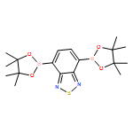
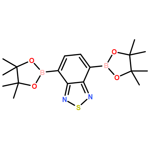


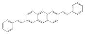


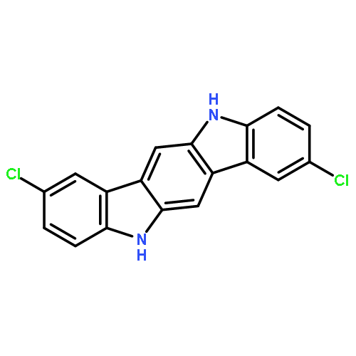


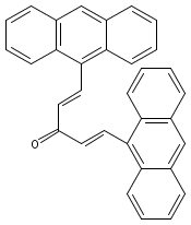
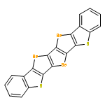
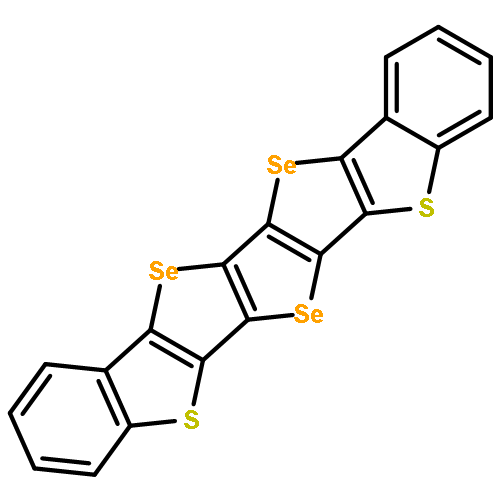

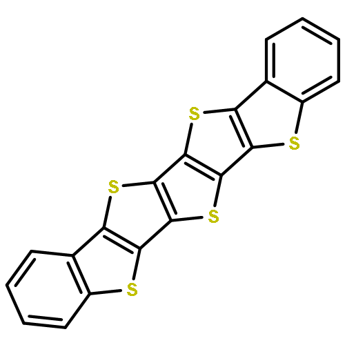
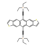
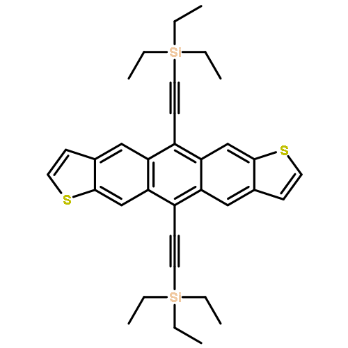
![1,3-dibromo-5-(n-dodecyl)thieno[3,4-c]pyrrole-4,6-dione](http://img.cochemist.com/ccimg/773900/773881-47-3.png)
![1,3-dibromo-5-(n-dodecyl)thieno[3,4-c]pyrrole-4,6-dione](http://img.cochemist.com/ccimg/773900/773881-47-3_b.png)
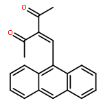


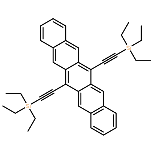
![Benzo[lmn][3,8]phenanthroline-1,3,6,8(2H,7H)-tetrone, 2,7-bis(2,2,3,3,4,4,4-heptafluorobutyl)-](/data/chemimg/136100/268724-95-4.png)
![Benzo[lmn][3,8]phenanthroline-1,3,6,8(2H,7H)-tetrone, 2,7-bis(2,2,3,3,4,4,4-heptafluorobutyl)-](/data/chemimg/136100/268724-95-4_b.png)


![Stannane, tributyl[2,2':5',2''-terthiophen]-5-yl-](http://img.cochemist.com/ccimg/214100/214044-46-9.png)
![Stannane, tributyl[2,2':5',2''-terthiophen]-5-yl-](http://img.cochemist.com/ccimg/214100/214044-46-9_b.png)


![2,6-Diiodobenzo[1,2-b:4,5-b']dithiophene](http://img.cochemist.com/ccimg/156000/155904-20-4.png)
![2,6-Diiodobenzo[1,2-b:4,5-b']dithiophene](http://img.cochemist.com/ccimg/156000/155904-20-4_b.png)


![Propanenitrile,3,3'-[[2-[4,5-bis[(2-cyanoethyl)thio]-1,3-dithiol-2-ylidene]-1,3-dithiole-4,5-diyl]bis(thio)]bis-](http://img.cochemist.com/ccimg/132800/132765-36-7.png)
![Propanenitrile,3,3'-[[2-[4,5-bis[(2-cyanoethyl)thio]-1,3-dithiol-2-ylidene]-1,3-dithiole-4,5-diyl]bis(thio)]bis-](http://img.cochemist.com/ccimg/132800/132765-36-7_b.png)


![Anthra[2,1,9-def:6,5,10-d'e'f']diisoquinoline-1,3,8,10(2H,9H)-tetrone,5,6,12,13-tetrachloro-](/data/chemimg/102600/115662-06-1.png)
![Anthra[2,1,9-def:6,5,10-d'e'f']diisoquinoline-1,3,8,10(2H,9H)-tetrone,5,6,12,13-tetrachloro-](/data/chemimg/102600/115662-06-1_b.png)


![Anthra[2,1,9-def:6,5,10-d'e'f']diisoquinoline-1,3,8,10(2H,9H)-tetrone,2,9-ditridecyl-](http://img.cochemist.com/ccimg/95700/95689-92-2.png)
![Anthra[2,1,9-def:6,5,10-d'e'f']diisoquinoline-1,3,8,10(2H,9H)-tetrone,2,9-ditridecyl-](http://img.cochemist.com/ccimg/95700/95689-92-2_b.png)
![3,7-dibromodibenzo[b,d]thiophene 5,5-dioxide](http://img.cochemist.com/ccimg/83900/83834-12-2.png)
![3,7-dibromodibenzo[b,d]thiophene 5,5-dioxide](http://img.cochemist.com/ccimg/83900/83834-12-2_b.png)
![Anthra[2,1,9-def:6,5,10-d'e'f']diisoquinoline-1,3,8,10(2H,9H)-tetrone, 2,9-bis[2,6-bis(1-methylethyl)phenyl]-](/data/chemimg/2251000/82953-57-9.png)
![Anthra[2,1,9-def:6,5,10-d'e'f']diisoquinoline-1,3,8,10(2H,9H)-tetrone, 2,9-bis[2,6-bis(1-methylethyl)phenyl]-](/data/chemimg/2251000/82953-57-9_b.png)
![THIENO[3,4-D]-1,3-DITHIOLE, 2-THIENO[3,4-D]-1,3-DITHIOL-2-YLIDENE-](http://img.cochemist.com/ccimg/80300/80229-45-4.png)
![THIENO[3,4-D]-1,3-DITHIOLE, 2-THIENO[3,4-D]-1,3-DITHIOL-2-YLIDENE-](http://img.cochemist.com/ccimg/80300/80229-45-4_b.png)
![Anthra[2,1,9-def:6,5,10-d'e'f']diisoquinoline-1,3,8,10(2H,9H)-tetrone, 2,9-dioctyl-](/data/chemimg/709500/78151-58-3.png)
![Anthra[2,1,9-def:6,5,10-d'e'f']diisoquinoline-1,3,8,10(2H,9H)-tetrone, 2,9-dioctyl-](/data/chemimg/709500/78151-58-3_b.png)


![2,7-dioctylbenzo[lmn][3,8]phenanthroline-1,3,6,8(2H,7H)-tetraone](http://img.cochemist.com/ccimg/34200/34155-21-0.png)
![2,7-dioctylbenzo[lmn][3,8]phenanthroline-1,3,6,8(2H,7H)-tetraone](http://img.cochemist.com/ccimg/34200/34155-21-0_b.png)


![DIINDENO[1,2-B:2',1'-D]THIOPHENE, 10,11-DIHYDRO-](http://img.cochemist.com/ccimg/7100/7099-33-4.png)
![DIINDENO[1,2-B:2',1'-D]THIOPHENE, 10,11-DIHYDRO-](http://img.cochemist.com/ccimg/7100/7099-33-4_b.png)


![Thieno[3,2-b:4,5-b']bis[1]benzothiophene](http://img.cochemist.com/ccimg/300/241-13-4.png)
![Thieno[3,2-b:4,5-b']bis[1]benzothiophene](http://img.cochemist.com/ccimg/300/241-13-4_b.png)
![Stannane, 1,1'-[4,8-bis(dodecyloxy)benzo[1,2-b:4,5-b']dithiophene-2,6-diyl]bis[1,1,1-trimethyl-](/data/chemimg/139400/1044795-08-5.png)
![Stannane, 1,1'-[4,8-bis(dodecyloxy)benzo[1,2-b:4,5-b']dithiophene-2,6-diyl]bis[1,1,1-trimethyl-](/data/chemimg/139400/1044795-08-5_b.png)

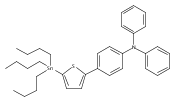
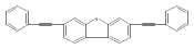


![Anthra[2,1,9-def:6,5,10-d'e'f']diisoquinoline-1,3,8,10(2H,9H)-tetrone, 5,6,12,13-tetrachloro-2,9-dioctyl-](/data/chemimg/3784400/95689-65-9.png)
![Anthra[2,1,9-def:6,5,10-d'e'f']diisoquinoline-1,3,8,10(2H,9H)-tetrone, 5,6,12,13-tetrachloro-2,9-dioctyl-](/data/chemimg/3784400/95689-65-9_b.png)


![[2]Benzopyrano[6,5,4-def][2]benzopyran-1,3,6,8-tetrone, 4,9-dibromo-](/data/chemimg/1015800/83204-68-6.png)
![[2]Benzopyrano[6,5,4-def][2]benzopyran-1,3,6,8-tetrone, 4,9-dibromo-](/data/chemimg/1015800/83204-68-6_b.png)


![Thieno[2,3-b:5,4-b']bis[1]benzothiophene](http://img.cochemist.com/ccimg/200/198-50-5.png)
![Thieno[2,3-b:5,4-b']bis[1]benzothiophene](http://img.cochemist.com/ccimg/200/198-50-5_b.png)


![23,24,25,26-Tetrathiapentacyclo[18.2.1.13,6.19,12.114,17]hexacosa-1,3,5,7,9,11,13,15,17,19,21-undecaene, 2,13-diphenyl-](/data/chemimg/3777500/1265748-61-5.png)
![23,24,25,26-Tetrathiapentacyclo[18.2.1.13,6.19,12.114,17]hexacosa-1,3,5,7,9,11,13,15,17,19,21-undecaene, 2,13-diphenyl-](/data/chemimg/3777500/1265748-61-5_b.png)