Co-reporter:Yunlong Xu, Xifeng Li, Leyong Zhu, Jianhua Zhang
Materials Science in Semiconductor Processing 2016 Volume 46() pp:23-28
Publication Date(Web):May 2016
DOI:10.1016/j.mssp.2016.02.001
The properties of solution-processed Al2O3 thin films annealed at different temperatures were thoroughly studied through thermogravimetry–differential thermal analysis, UV–vis-NIR spectrophotometer measurements, scanning electron microscopy, X-ray diffraction, atomic force microscopy and a series of electrical measurements. The solution-processed ZnInSnO thin films transistors (TFTs) with the prepared Al2O3 dielectric were annealed at different temperatures. The TFTs annealed at 600 °C have displayed excellent electrical performance such as the field-effect mobility of 116.9 cm2 V−1 s−1 and a subthreshold slope of 93.3 mV/dec. The performance of TFT device could be controlled by adjusting the annealing temperature. The results of two-dimensional device simulations demonstrate that the improvement of device performance are closely related with the reduction of interface defects between channel and dielectric and subgap density of stats (DOS) in the channel layer.
Co-reporter:Y. N. Gao, Y. L. Xu, J. G. Lu, J. H. Zhang and X. F. Li
Journal of Materials Chemistry A 2015 vol. 3(Issue 43) pp:11497-11504
Publication Date(Web):06 Oct 2015
DOI:10.1039/C5TC02485D
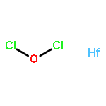
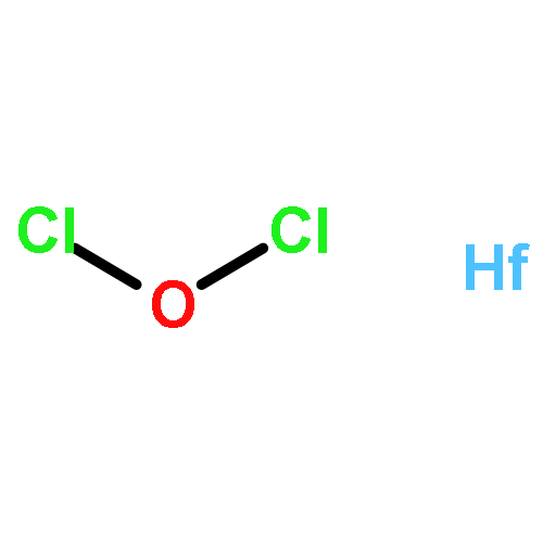
Novel solution-processed amorphous high-k dielectrics for thin film transistors (TFTs) have been systemically studied with the objective of achieving high performance and reducing costs for the next generation displays. In this research, amorphous hafnium silicon multiple oxide (HfSiOx) was fabricated by a simple spin-coating method. Here, we have demonstrated that the incorporation of a silicon oxide has significant effects on the properties of HfO2. The HfSiOx dielectrics had no obvious crystallization peaks even when the annealing temperature reached up to 800 °C while the HfO2 films were crystallized at 400 °C. The HfSiOx films had an energy band gap of 6.05 eV, which was wider than HfO2 films (5.69 eV), the breakdown voltage increased from 2.4 MV cm−1 (HfO2) to 2.9 MV cm−1 (HfSiOx) and the leakage current decreased from 4.4 × 10⁻⁷ A cm−2 to 3.7 × 10⁻⁷ A cm−2 at an electric field of 2 MV cm−1. To achieve optimized device performance, the influence of annealing temperature on the characteristics (including the surface and interface, the chemical and structural evolution) of the solution processed HfSiOx dielectrics was emphasized in this research. To demonstrate the HfSiOx application in oxide TFTs, we fabricated HfInZnO (HIZO) and ZnSnO (ZTO) TFTs with HfSiOx dielectrics, and both of them showed low off-state current indicating HfSiOx is an attractive candidate used in TFTs. The ZTO TFTs with amorphous HfSiOx dielectrics operated well under a gate voltage of −0.53 V, exhibiting a high saturation mobility of 153 cm2 V−1 s−1, a small subthreshold swing of 0.17 V dec−1, and a large on–off current ratio 3.4 × 10⁷.
Co-reporter:Jianhua Zhang, Panpan Dong, Yana Gao, Chenhang Sheng, and Xifeng Li
ACS Applied Materials & Interfaces 2015 Volume 7(Issue 43) pp:24103
Publication Date(Web):October 16, 2015
DOI:10.1021/acsami.5b07148
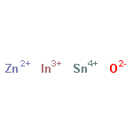
In this article, we reported the stacked structure zinc–indium-tin oxide (ZITO) thin-film transistors (TFTs) with graphene nanosheets (GNSs) prepared by solution process. GNSs were used as bridge layer between dual-ZITO layers. The transmission of stacked ZITO/GNSs/ZITO films are more than 80% in the visible region and the resistivity of ZITO films with GNSs bridge layer decreased from 502.9 to 13.4 Ω cm. The solution-processed TFT devices with GNSs bridge layer exhibited a desirable characteristic with a subthreshold slope of 0.25 V/dec and current on–off ratio of 1 × 10⁷, and the saturation filed effect mobility is improved to 45.9 cm2V–1s–1, which exceeds the mobility values of the pristine ZITO TFTs by one order. These results demonstrate the solution-processed ZITO/GNSs/ZITO TFTs maybe make a further step to achieve high-performance TFTs and show the potential for next-generation applications.Keywords: bridge layer; graphene; sol−gel; thin film transistors; ZITO
Co-reporter:Yana Gao, Jianguo Lu, Jianhua Zhang and Xifeng Li
RSC Advances 2015 vol. 5(Issue 47) pp:37635-37639
Publication Date(Web):17 Apr 2015
DOI:10.1039/C5RA01800E
The energy band tailoring of indium zinc oxide (IZO) through Al incorporation was studied and measured directly by ultraviolet photoelectron spectroscopy (UPS). Al doped IZO (AIZO) thin films have lower work function (3.90 eV) and wider bandgap (3.75 eV) compared with IZO (4.15 and 3.5 eV, respectively). These changes induced by Al incorporation would result in higher activation energy and higher flat voltage for AIZO TFTs, which may imply the origin of the AIZO TFTs electrical properties such as threshold voltage shift and off-state current decrease.
Co-reporter:Juan Peng;Chenhang Sheng;Jifeng Shi
Journal of Sol-Gel Science and Technology 2014 Volume 71( Issue 3) pp:458-463
Publication Date(Web):2014 September
DOI:10.1007/s10971-014-3400-y
In this paper, high-k titanium–aluminum oxide (ATO) dielectric film has been realized by using organic–inorganic hybrid precursor solution. X-ray diffraction pattern revealed that the ATO films (Ti content less than 67 at%) remain amorphous phase for annealing treatment at 400 °C. And all of the amorphous ATO films had very smooth and uniform surface with root mean square (RMS) roughness of less than 0.5 nm. Meanwhile, the results showed that the ATO film (Ti:Al = 1:8) had the best performance, including RMS roughness of 0.33 nm, relative permittivity of 15, and leakage current density of 1.41 × 10⁻⁶ A/cm2 at 1 MV/cm.
Co-reporter:Xifeng Li, Enlong Xin, Longlong Chen, Jifeng Shi, Chunya Li, Jianhua Zhang
Materials Science in Semiconductor Processing 2013 Volume 16(Issue 5) pp:1292-1296
Publication Date(Web):October 2013
DOI:10.1016/j.mssp.2013.02.013
Co-reporter:Xifeng Li;Qian Li;Jianhua Zhang
Journal of Sol-Gel Science and Technology 2013 Volume 66( Issue 3) pp:497-503
Publication Date(Web):2013 June
DOI:10.1007/s10971-013-3037-2
Transparent amorphous Indium-Gallium-Zinc-oxide thin films transistors (a-IGZO TFTs) were fabricated using spin-coating technique at a relative low annealing temperature of 300 °C. The effects of the gallium (Ga) concentration on the properties of the IGZO solutions, the optical properties of the a-IGZO films,and the a-IGZO TFTs device properties were researched. The a-IGZO thin films were uniform and smooth, root mean square roughness of IGZO films was less than 0.4 nm, and the transmittance was more than 80 % in the visible wavelength. The results showed that An appropriate amount of Ga doping and annealing temperature could significant improve the a-IGZO TFTs’ device performance. A saturation mobility of 0.04 cm2 V−1 s−1 was obtained when the Ga concentration reached 10.7 %.
Co-reporter:Xifeng Li;Qian Li;Enlong Xin;Jianhua Zhang
Journal of Sol-Gel Science and Technology 2013 Volume 65( Issue 2) pp:130-134
Publication Date(Web):2013 February
DOI:10.1007/s10971-012-2916-2
Indium–zinc oxide (IZO) thin films were fabricated by spin coating using acetate- and nitrate-based precursors, and thin film transistors (TFTs) were further fabricated employing the IZO films as the active channel layer. The impact of the indium concentration on the properties of the solutions, the structure and optical transmittance properties of the IZO films and the IZO TFTs device properties were researched in this article. The IZO films with amorphous structure were obtained when the annealing temperature is 500 °C. The transmittance could reach ~90 % (including glass substrate) during the visible region of 400–760 nm. Higher indium concentration can improve the IZO TFTs’ filed effect mobility. A Ion–Ioff of 6.0 × 10⁶ and a mobility of 0.13 cm2/Vs were obtained when the indium concentration is 60 %. IZO TFTs’ performance could deteriorate when the indium concentration more than 60 %.
Co-reporter:Ji-feng Shi 李继锋;Long-long Chen 陈龙龙
Journal of Shanghai University (English Edition) 2011 Volume 15( Issue 4) pp:
Publication Date(Web):2011 August
DOI:10.1007/s11741-011-0729-1
Amorphous InGaZnO (a-IGZO) films were deposited on the corning eagle XG (EXG) glass substrates using magnetron sputtering method. The structure, surface morphology, electrical and optical properties of these films were investigated by X-ray diffraction (XRD), scanning electron microscopy (SEM), semiconductor parameter analyzer and spectrophotometry, respectively. The influence of oxygen flow on the electrical properties of IGZO thin films was studied, showing that increasing oxygen flow changes the resistivity with six orders of magnitude. The contact resistance of ITO/IGZO is 7.35×10⁻² Ω·cm2, which suggests that a good ohmic contact exists between In2O3: Sn (ITO) and IGZO film.
Co-reporter:Long-long Chen 陈龙龙;Ji-feng Shi 石继锋
Journal of Shanghai University (English Edition) 2011 Volume 15( Issue 4) pp:
Publication Date(Web):2011 August
DOI:10.1007/s11741-011-0730-1
Amorphous InGaZnO (a-IGZO) film is deposited on the glass substrate by radio-frequency sputtering and the influence of annealing on wet etch of a-IGZO films were investigated. The results show that etch rate of IGZO films decrease with the increase of annealing temperature. Etching taper angle is less than 60° and critical dimension (CD) loss is less than 1 μm in over-etching time of 30 s. The fact implies that IGZO films etching with oxalic acid may be a good wet etching way for the thin-film transistor (TFT) array process.
Co-reporter:Y. N. Gao, Y. L. Xu, J. G. Lu, J. H. Zhang and X. F. Li
Journal of Materials Chemistry A 2015 - vol. 3(Issue 43) pp:NaN11504-11504
Publication Date(Web):2015/10/06
DOI:10.1039/C5TC02485D
Novel solution-processed amorphous high-k dielectrics for thin film transistors (TFTs) have been systemically studied with the objective of achieving high performance and reducing costs for the next generation displays. In this research, amorphous hafnium silicon multiple oxide (HfSiOx) was fabricated by a simple spin-coating method. Here, we have demonstrated that the incorporation of a silicon oxide has significant effects on the properties of HfO2. The HfSiOx dielectrics had no obvious crystallization peaks even when the annealing temperature reached up to 800 °C while the HfO2 films were crystallized at 400 °C. The HfSiOx films had an energy band gap of 6.05 eV, which was wider than HfO2 films (5.69 eV), the breakdown voltage increased from 2.4 MV cm−1 (HfO2) to 2.9 MV cm−1 (HfSiOx) and the leakage current decreased from 4.4 × 10⁻⁷ A cm−2 to 3.7 × 10⁻⁷ A cm−2 at an electric field of 2 MV cm−1. To achieve optimized device performance, the influence of annealing temperature on the characteristics (including the surface and interface, the chemical and structural evolution) of the solution processed HfSiOx dielectrics was emphasized in this research. To demonstrate the HfSiOx application in oxide TFTs, we fabricated HfInZnO (HIZO) and ZnSnO (ZTO) TFTs with HfSiOx dielectrics, and both of them showed low off-state current indicating HfSiOx is an attractive candidate used in TFTs. The ZTO TFTs with amorphous HfSiOx dielectrics operated well under a gate voltage of −0.53 V, exhibiting a high saturation mobility of 153 cm2 V−1 s−1, a small subthreshold swing of 0.17 V dec−1, and a large on–off current ratio 3.4 × 10⁷.

![1,4-Benzenediamine, N1-2-naphthalenyl-N4,N4-bis[4-(2-naphthalenylphenylamino)phenyl]-N1-phenyl-](/data/chemimg/104700/185690-41-9.png)
![1,4-Benzenediamine, N1-2-naphthalenyl-N4,N4-bis[4-(2-naphthalenylphenylamino)phenyl]-N1-phenyl-](/data/chemimg/104700/185690-41-9_b.png)
![Bisbenz[5,6]indeno[1,2,3-cd:1',2',3'-lm]perylene, 5,10,15,20-tetraphenyl-](/data/chemimg/116100/175606-05-0.png)
![Bisbenz[5,6]indeno[1,2,3-cd:1',2',3'-lm]perylene, 5,10,15,20-tetraphenyl-](/data/chemimg/116100/175606-05-0_b.png)