Co-reporter:Kai-Lin Ou, Ramanan Ehamparam, Gordon MacDonald, Tobias Stubhan, Xin Wu, R. Clayton Shallcross, Robin Richards, Christoph J. Brabec, S. Scott Saavedra, and Neal R. Armstrong
ACS Applied Materials & Interfaces 2016 Volume 8(Issue 30) pp:19787-19798
Publication Date(Web):June 30, 2016
DOI:10.1021/acsami.6b02792
This report focuses on the evaluation of the electrochemical properties of both solution-deposited sol–gel (sg-ZnO) and sputtered (sp-ZnO) zinc oxide thin films, intended for use as electron-collecting interlayers in organic solar cells (OPVs). In the electrochemical studies (voltammetric and impedance studies), we used indium–tin oxide (ITO) over coated with either sg-ZnO or sp-ZnO interlayers, in contact with either plain electrolyte solutions, or solutions with probe redox couples. The electroactive area of exposed ITO under the ZnO interlayer was estimated by characterizing the electrochemical response of just the oxide interlayer and the charge transfer resistance from solutions with the probe redox couples. Compared to bare ITO, the effective electroactive area of ITO under sg-ZnO films was ca. 70%, 10%, and 0.3% for 40, 80, and 120 nm sg-ZnO films. More compact sp-ZnO films required only 30 nm thicknesses to achieve an effective electroactive ITO area of ca. 0.02%. We also examined the electrochemical responses of these same ITO/ZnO heterojunctions overcoated with device thickness pure poly(3-hexylthiophehe) (P3HT), and donor/acceptor blended active layers (P3HT:PCBM). Voltammetric oxidation/reduction of pure P3HT thin films on ZnO/ITO contacts showed that pinhole pathways exist in ZnO films that permit dark oxidation (ITO hole injection into P3HT). In P3HT:PCBM active layers, however, the electrochemical activity for P3HT oxidation is greatly attenuated, suggesting PCBM enrichment near the ZnO interface, effectively blocking P3HT interaction with the ITO contact. The shunt resistance, obtained from dark current–voltage behavior in full P3HT/PCBM OPVs, was dependent on both (i) the porosity of the sg-ZnO or sp-ZnO films (as revealed by probe molecule electrochemistry) and (ii) the apparent enrichment of PCBM at ZnO/P3HT:PCBM interfaces, both effects conveniently revealed by electrochemical characterization. We anticipate that these approaches will be applicable to a wider array of solution-processed interlayers for “printable” solar cells.
Co-reporter:Ramanan Ehamparam, Nicholas G. Pavlopoulos, Michael W. Liao, Lawrence J. Hill, Neal R. Armstrong, Jeffrey Pyun, and S. Scott Saavedra
ACS Nano 2015 Volume 9(Issue 9) pp:8786
Publication Date(Web):August 20, 2015
DOI:10.1021/acsnano.5b01720
Conduction and valence band energies (ECB, EVB) for CdSe nanorods (NRs) functionalized with Au nanoparticle (NP) tips are reported here, referenced to the vacuum scale. We use (a) UV photoemission spectroscopy (UPS) to measure EVB for NR films, utilizing advanced approaches to secondary electron background correction, satellite removal to enhance spectral contrast, and correction for shifts in local vacuum levels; and (b) waveguide-based spectroelectrochemistry to measure ECB from onset potentials for electron injection into NR films tethered to ITO. For untipped CdSe NRs, both approaches show EVB = 5.9–6.1 eV and ECB = 4.1–4.3 eV. Addition of Au tips alters the NR band edge energies and introduces midgap states, in ways that are predicted to influence the efficiency of these nanomaterials as photoelectrocatalysts. UPS results show that Au tipping shifts EVB closer to vacuum by up to 0.4 eV, shifts the apparent Fermi energy toward the middle of the band gap, and introduces additional states above EVB. Spectroelectrochemical results confirm these trends: Au tipping shifts ECB closer to vacuum, by 0.4–0.6 eV, and introduces midgap states below ECB, which are assigned as metal–semiconductor interface (MSI) states. Characterization of these band edge energies and understanding the origins of MSI states is needed to design energy conversion systems with proper band alignment between the light absorbing NR, the NP catalyst, and solution electron donors and acceptors. The complementary characterization protocols presented here should be applicable to a wide variety of thin films of heterogeneous photoactive nanomaterials, aiding in the identification of the most promising material combinations for photoelectrochemical energy conversion.Keywords: band edge energies; electron transfer; metal nanoparticle; semiconductor nanorods; spectroelectrochemistry; UV photoemission;
Co-reporter:R. Clayton Shallcross; Tobias Stubhan; Erin L. Ratcliff; Antoine Kahn; Christoph J. Brabec
The Journal of Physical Chemistry Letters 2015 Volume 6(Issue 8) pp:1303-1309
Publication Date(Web):March 24, 2015
DOI:10.1021/acs.jpclett.5b00444
We demonstrate new approaches to the characterization of oxidized regioregular poly(3-hexylthiophene-2,5-diyl) (P3HT) that results from electronic equilibration with device-relevant high work function electrical contacts using high-resolution X-ray (XPS) and ultraviolet (UPS) photoelectron spectroscopy (PES). Careful interpretation of photoemission signals from thiophene sulfur atoms in thin (ca. 20 nm or less) P3HT films provides the ability to uniquely elucidate the products of charge transfer between the polymer and the electrical contact, which is a result of Fermi-level equilibration between the two materials. By comparing high-resolution S 2p core-level spectra to electrochemically oxidized P3HT standards, the extent of the contact doping reaction is quantified, where one in every six thiophene units (ca. 20%) in the first monolayer is oxidized. Finally, angle-resolved XPS of both pure P3HT and its blends with phenyl-C61-butyric acid methyl ester (PCBM) confirms that oxidized P3HT species exist near contacts with work functions greater than ca. 4 eV, providing a means to characterize the interface and “bulk” region of the organic semiconductor in a single film.
Co-reporter:Graham E. Morse, Jeremy L. Gantz, K. Xerxes Steirer, Neal R. Armstrong, and Timothy P. Bender
ACS Applied Materials & Interfaces 2014 Volume 6(Issue 3) pp:1515
Publication Date(Web):December 27, 2013
DOI:10.1021/am404179z
We have demonstrated that pentafluoro phenoxy boron subphthalocyanine (F5BsubPc) can function as either an electron donor or an electron acceptor layer in a planar heterojunction organic photovolatic (PHJ OPV) cell. F5BsubPc was incorporated into devices with the configurations ITO/MoO3/F5BsubPc/C60/BCP/Al (F5BsubPc used as an electron-donor/hole-transport layer) and ITO/MoO3/Cl-BsubPc/F5BsubPc/BCP/Al (F5BsubPc used as an electron-acceptor/electron-transport layer). Each unoptimized device displayed open-circuit photopotentials (Voc) close to or in excess of 1 V and respectrable power conversion efficiencies. Ultraviolet photoelectron spectroscopy (UPS) was used to characterize the band-edge offset energies at the donor/acceptor junctions. HOMO and LUMO energy level offsets for the F5BsubPc/C60 heterojunction were determined to be ca. 0.6 eV and ca. 0.7 eV, respectively. Such offsets are clearly large enough to produce rectifying J/V responses, efficient exciton dissociation, and photocurrent production at the interface. For the Cl-BsubPc/F5BsubPc heterojunction, the estimated offset energies were found to be ca. 0.1 eV. However, reasonable photovoltaic activity was observed, with photocurrent production coming from both BsubPc species layers. Incident and absorbed photon power conversion efficiencies (IPCE and APCE) showed that photocurrent production qualitatively tracked the absorbance spectra of the donor/acceptor heterojunctions, with some additional photocurrent activity on the low energy side of the absorbance band. We suggest that photocurrent production at higher wavelengths may be a result of charge-transfer species at the donor/acceptor interface. Cascade photovoltaics were also fabricated to expand on the understanding of the role of F5BsubPc in such device architectures.Keywords: boron; cells; heterojunctions; photovoltaic; solar; subphthalocyanines;
Co-reporter:Kai-Lin Ou, Delvin Tadytin, K. Xerxes Steirer, Diogenes Placencia, Mike Nguyen, Paul Lee and Neal R. Armstrong
Journal of Materials Chemistry A 2013 vol. 1(Issue 23) pp:6794-6803
Publication Date(Web):26 Apr 2013
DOI:10.1039/C3TA10894E
We demonstrate the use of chemical vapor deposition (CVD) to create unique thin (12–36 nm) and conformal TiO2 interlayers on indium-tin oxide (ITO) electrodes, for use as electron collection contacts in inverted bulk heterojunction P3HT/PC61BM organic photovoltaics (OPVs). Optimized CVD formation of these oxide films is inherently scalable to large areas, and may be a viable non-contact alternative to electron-selective interlayer formation. Oxide-based electron-selective interlayers, such as TiO2, need to be thin, conformal and sufficiently electronically conducting films without sacrificing electron harvesting selectivity. Using volatile titanium-tetraisopropoxide (TTIP) precursors in a flowing N2 gas stream, the CVD process provides nanometer control of film thickness to produce 12–36 nm thickness device-quality films. The best performing CVD films, processed at substrate temperatures of ca. 210 °C, characterized using X-ray diffraction (XRD) and X-ray photoelectron spectroscopy (XPS) were found to be amorphous but stoichiometric TiO2. Solution electrochemistries (voltammetry) of probe molecules were shown to be easily accessible indicators of film porosity and are predictive for electron harvesting selectivity (and hole-blocking) in an inverted configuration OPV platform. Small molecules whose redox potentials placed them energetically above the conduction band edge energy (ECB) were reduced/oxidized at nearly the same rates as for bare ITO. Probe molecules whose redox potentials place them energetically within the band gap region, below ECB, show almost complete blocking of their oxidation/reduction processes, for optimized conformal (and nonporous) TiO2 films. In addition, background oxidation current densities for solution probe molecules correlate inversely with the shunt resistance (RP) measured in OPVs. OPVs with the configuration: ITO/CVD-TiO2/P3HT:PC61BM/MoO3/Ag, using TiO2 films of 12, 24 and 36 nm, were evaluated for short-circuit photocurrent (JSC), open-circuit photopotential (VOC), and fill-factor (FF), versus bare ITO. OPVs using amorphous, conformal 24 nm TiO2 interlayers showed the highest fill factors, lowest RS, highest RP and power conversion efficiencies of ca. 3.7%.
Co-reporter:K. Xerxes Steirer ; Gordon A. MacDonald ; Selina Olthof ; Jeremy Gantz ; Erin L. Ratcliff ; Antoine Kahn
The Journal of Physical Chemistry C 2013 Volume 117(Issue 43) pp:22331-22340
Publication Date(Web):July 3, 2013
DOI:10.1021/jp402672j
We present the interface characterization of vacuum-deposited metal nanoparticle recombination layers (Ag, Au; 1 nm equivalent thickness) at donor/acceptor heterojunctions comprising copper phthalocyanine (CuPc) and C60 as model interfaces for tandem planar heterojunction organic photovoltaics (TOPVs). We compare the extent to which voltage doubling occurs using these two metal recombination contacts (RC) in TOPVs (ITO/CuPc/C60/(Ag,Au)/CuPc/C60/BCP/Al) and correlate the differences with energetic dissimilarities revealed by UV-photoemission (UPS) and inverse photoemission (IPES) spectroscopies, and morphology as revealed by atomic force microscopy (AFM) and field-emission scanning electron microscopy (FE-SEM). Ag interlayer RCs produce the expected voltage doubling in the open-circuit voltage (VOC) for the TOPV, whereas Au RCs showed poor voltage addition. Significant shifts in ionization potential and electron affinity and shifts in local work function were observed for C60/metal heterojunctions and for heterojunctions based on C60/metal/C60 and for C60/metal/CuPc, with clear evidence for partial charge redistribution between C60 and Ag nanoparticles. AFM and FE-SEM images revealed discrete Ag nanoparticles at the C60 interface, whereas Au/C60 heterojunctions consisted of more uniform Au thin films that wet the C60 surface and penetrated below the surface. These studies point to the need for careful control of both electronic and morphological properties of thin RCs in emerging tandem organic solar cell technologies.
Co-reporter:Jeremy Gantz, Diogenes Placencia, Anthony Giordano, Seth R. Marder, and Neal R. Armstrong
The Journal of Physical Chemistry C 2013 Volume 117(Issue 3) pp:1205-1216
Publication Date(Web):December 19, 2012
DOI:10.1021/jp307546v
We present a systematic study of the band-edge energy offsets and shifts in local vacuum levels for indium tin oxide (ITO)/donor heterojunctions, using vacuum-deposited chloroindium phthalocyanine (ClInPc), titanyl phthalocyanine (TiOPc), pentacene (PEN), and copper phthalocyanine (CuPc) donor layers. We include a comparison of the performance of ITO/donor/C60 planar heterojunction (PHJ) organic solar cells (OPVs) as a function of activation and modification of the ITO contact. UV photoemission spectroscopy (UPS) was used to characterize the interfacial region between these donors and ITO to infer the ordering of these first deposited 1–2 monolayers as a function of ITO activation and modification. For the polar donors ClInPc and TiOPc, deposited on air plasma (AP) treated, high work function ITO (φeff ≈ 5.1–5.2 eV), shifts in local vacuum level observed during deposition of the first two monolayers of donor molecules suggest that the halo–metal or oxo–metal bond points (on average) toward the oxide surface in the first monolayer. Inversion of this orientation is inferred during formation of the second monolayer. Thin-film absorbance data for the Q-band spectra of ClInPc or TiOPc 1–2 monolayers on AP-ITO confirmed the organization of the first deposited layers. Use of nonactivated ITO contacts, or contacts modified with pentafluorobenzylphosphonic acid (F5BPA), disrupts this order in the first two monolayers as revealed in the UPS and absorbance data, leading to decreases in OPV open-circuit photopotential (VOC), fill factor (FF), and efficiency (η). For nonpolar donors like PEN and CuPc, shifts in local vacuum level as a function of donor coverage were less sensitive to ITO surface composition, and PEN-based OPVs show relatively invariant VOC, JSC, FF, and η values regardless of ITO pretreatment or F5BPA modification.The interaction of ClInPc donor layers with AP-ITO is strong enough to generate photovoltaic activity in the absence of a C60 acceptor layer (ITO/ClInPc/Al device configurations), where photocurrent appears to be generated at the ITO/ClInPc interface. Such an effect is not seen for ITO/ClInPc/Al devices on nonactivated ITO substrates, highlighting the importance of the interactions between the donor layer and the hole-harvesting interface in PHJ OPVs. These results suggest that the organization of a dipolar donor layer at a hole-harvesting oxide contact can affect OPV performance where charge harvesting efficiency is sensitive to molecular organization in the interfacial region near the contact.
Co-reporter:Peter J. Hotchkiss, Simon C. Jones, Sergio A. Paniagua, Asha Sharma, Bernard Kippelen, Neal R. Armstrong, and Seth R. Marder
Accounts of Chemical Research 2012 Volume 45(Issue 3) pp:337
Publication Date(Web):October 19, 2011
DOI:10.1021/ar200119g
Transparent metal oxides, in particular, indium tin oxide (ITO), are critical transparent contact materials for applications in next-generation organic electronics, including organic light emitting diodes (OLEDs) and organic photovoltaics (OPVs). Understanding and controlling the surface properties of ITO allows for the molecular engineering of the ITO–organic interface, resulting in fine control of the interfacial chemistries and electronics. In particular, both surface energy matching and work function compatibility at material interfaces can result in marked improvement in OLED and OPV performance. Although there are numerous ways to change the surface properties of ITO, one of the more successful surface modifications is the use of monolayers based on organic molecules with widely variable end functional groups. Phosphonic acids (PAs) are known to bind strongly to metal oxides and form robust monolayers on many different metal oxide materials. They also demonstrate several advantages over other functionalizing moieties such as silanes or carboxylic acids. Most notably, PAs can be stored in ambient conditions without degradation, and the surface modification procedures are typically robust and easy to employ.This Account focuses on our research studying PA binding to ITO, the tunable properties of the resulting surfaces, and subsequent effects on the performance of organic electronic devices. We have used surface characterization techniques such as X-ray photoelectron spectroscopy (XPS) and infrared reflection adsorption spectroscopy (IRRAS) to determine that PAs bind to ITO in a predominantly bidentate fashion (where two of three oxygen atoms from the PA are involved in surface binding). Modification of the functional R-groups on PAs allows us to control and tune the surface energy and work function of the ITO surface. In one study using fluorinated benzyl PAs, we can keep the surface energy of ITO relatively low and constant but tune the surface work function. PA modification of ITO has resulted in materials that are more stable and more compatible with subsequently deposited organic materials, an effective work function that can be tuned by over 1 eV, and energy barriers to hole injection (OLED) or hole-harvesting (OPV) that can be well matched to the frontier orbital energies of the organic active layers, leading to better overall device properties.
Co-reporter:Gordon A. MacDonald, P. Alexander Veneman, Diogenes Placencia, and Neal R. Armstrong
ACS Nano 2012 Volume 6(Issue 11) pp:9623
Publication Date(Web):October 2, 2012
DOI:10.1021/nn303043y
We demonstrate mapping of electrical properties of heterojunctions of a molecular semiconductor (copper phthalocyanine, CuPc) and a transparent conducting oxide (indium–tin oxide, ITO), on 20–500 nm length scales, using a conductive-probe atomic force microscopy technique, scanning current spectroscopy (SCS). SCS maps are generated for CuPc/ITO heterojunctions as a function of ITO activation procedures and modification with variable chain length alkyl-phosphonic acids (PAs). We correlate differences in small length scale electrical properties with the performance of organic photovoltaic cells (OPVs) based on CuPc/C60 heterojunctions, built on these same ITO substrates. SCS maps the “ohmicity” of ITO/CuPc heterojunctions, creating arrays of spatially resolved current–voltage (J–V) curves. Each J–V curve is fit with modified Mott–Gurney expressions, mapping a fitted exponent (γ), where deviations from γ = 2.0 suggest nonohmic behavior. ITO/CuPc/C60/BCP/Al OPVs built on nonactivated ITO show mainly nonohmic SCS maps and dark J–V curves with increased series resistance (RS), lowered fill-factors (FF), and diminished device performance, especially near the open-circuit voltage. Nearly optimal behavior is seen for OPVs built on oxygen-plasma-treated ITO contacts, which showed SCS maps comparable to heterojunctions of CuPc on clean Au. For ITO electrodes modified with PAs there is a strong correlation between PA chain length and the degree of ohmicity and uniformity of electrical response in ITO/CuPc heterojunctions. ITO electrodes modified with 6–8 carbon alkyl-PAs show uniform and nearly ohmic SCS maps, coupled with acceptable CuPc/C60OPV performance. ITO modified with C14 and C18 alkyl-PAs shows dramatic decreases in FF, increases in RS, and greatly enhanced recombination losses.Keywords: conducting-tip atomic force microscopy; injection efficiency; ohmic contacts; organic semiconductor; organic solar cell
Co-reporter:Erin L. Ratcliff, Jens Meyer, K. Xerxes Steirer, Andres Garcia, Joseph J. Berry, David S. Ginley, Dana C. Olson, Antoine Kahn, and Neal R. Armstrong
Chemistry of Materials 2011 Volume 23(Issue 22) pp:4988
Publication Date(Web):October 26, 2011
DOI:10.1021/cm202296p
The characterization and implementation of solution-processed, wide bandgap nickel oxide (NiOx) hole-selective interlayer materials used in bulk-heterojunction (BHJ) organic photovoltaics (OPVs) are discussed. The surface electrical properties and charge selectivity of these thin films are strongly dependent upon the surface chemistry, band edge energies, and midgap state concentrations, as dictated by the ambient conditions and film pretreatments. Surface states were correlated with standards for nickel oxide, hydroxide, and oxyhydroxide components, as determined using monochromatic X-ray photoelectron spectroscopy. Ultraviolet and inverse photoemission spectroscopy measurements show changes in the surface chemistries directly impact the valence band energies. O2-plasma treatment of the as-deposited NiOx films was found to introduce the dipolar surface species nickel oxyhydroxide (NiOOH), rather than the p-dopant Ni2O3, resulting in an increase of the electrical band gap energy for the near-surface region from 3.1 to 3.6 eV via a vacuum level shift. Electron blocking properties of the as-deposited and O2-plasma treated NiOx films are compared using both electron-only and BHJ devices. O2-plasma-treated NiOx interlayers produce electron-only devices with lower leakage current and increased turn on voltages. The differences in behavior of the different pretreated interlayers appears to arise from differences in local density of states that comprise the valence band of the NiOx interlayers and changes to the band gap energy, which influence their hole-selectivity. The presence of NiOOH states in these NiOx films and the resultant chemical reactions at the oxide/organic interfaces in OPVs is predicted to play a significant role in controlling OPV device efficiency and lifetime.Keywords: interlayer; IPES; nickel oxide; OPV; organic solar cell; photoemission spectroscopy; selective contact; UPS; XPS;
Co-reporter:Weining Wang, Diogenes Placencia, Neal R. Armstrong
Organic Electronics 2011 Volume 12(Issue 2) pp:383-393
Publication Date(Web):February 2011
DOI:10.1016/j.orgel.2010.11.015
Planar and textured heterojunction solar cells (OPVs) are reported for vacuum deposited chloroindium phthalocyanine (ClInPc)/C60 heterojunctions, and their response compared to previously explored OPVs based on titanyl phthalocyanine (TiOPc)/C60 heterojunctions. As for TiOPc/C60 OPVs, the photoelectrical activity of ClInPc/C60 OPVs extends well into the near infrared, with good activity out to ca. 900 nm. As-deposited ClInPc films (Phase I) produce open-circuit photopotentials, VOC as high as ca. 0.8 V (Phase I form of ClInPc), ca. 0.15 V larger than previously observed for Phase I TiOPc/C60 OPVs. The offsets in frontier orbital energies (EHOMOPc–ELUMOC60) revealed by UV-photoemission studies (UPS) are slightly smaller for ClInPc/C60 versus TiOPc/C60 heterojunctions, and the interface dipole contribution (shift in local vacuum level) to these offsets is in the opposite direction for ClInPc/C60 versus TiOPc/C60 heterojunctions, or missing altogether, suggesting differences in molecular interaction at the Pc/C60 interface. Higher VOC values are correlated with lower reverse saturation currents, Jo, for ClInPc/C60, versus other Pc or pentacene/C60 heterojunctions, suggesting weak intermolecular interactions at the ClInPc/C60 interface and large barriers to dark charge injection. Solvent annealing of the ClInPc films enhances the near-IR response, and textures the Pc film, enhancing the Pc/C60 interfacial contact area and the short-circuit photocurrent, JSC. JSC under AM 1.5 illumination conditions was estimated by integration of the incident photon current efficiency (IPCE) response, to compare relative power conversion efficiencies for the two different device types. The estimated efficiency of Phase I ClInPc/C60 OPVs is ca. 2.6%. The estimated AM 1.5 efficiency of ClInPc/C60 OPVs with solvent annealed Pc layers is estimated to be ca. 3.3%, arising from the extensive texturing achieved of the Pc layer, which nearly doubles JSC for the Phase II versus Phase I Pc films.Graphical abstractWe demonstrate both planar and textured heterojunction organic solar cells (OPVs) based on chloro-indium phthalocyanine (ClInPc) as the donor layer. The near-IR absorptivity of this dye, coupled with its high ionization potential provides for good coverage of a critical spectral region, without sacrifice of open-circuit photopotential. Texturing via solvent annealing provides enhanced interfacial contact area between the donor Pc and the acceptor C60, providing OPV efficiencies up to 3.3%.Research highlights► Organic solar cells are introduced using chloro-indium phthalocyanine (ClInPc). ► ClInPc OPVs show a higher VOC than seen for most previous donors. ► ClInPc films are textured via solvent annealing to give higher JSC. ► ClInPc/C60 OPVs with textured donor layes show efficiencies in excess of 3%.
Co-reporter:Erin L. Ratcliff, Brian Zacher, and Neal R. Armstrong
The Journal of Physical Chemistry Letters 2011 Volume 2(Issue 11) pp:1337-1350
Publication Date(Web):May 23, 2011
DOI:10.1021/jz2002259
Organic photovoltaic cells (OPVs) are promising solar electric energy conversion systems with impressive recent optimization of active layers. OPV optimization must now be accompanied by the development of new charge-selective contacts and interlayers. This Perspective considers the role of interface science in energy harvesting using OPVs, looking back at early photoelectrochemical (photogalvanic) energy conversion platforms, which suffered from a lack of charge carrier selectivity. We then examine recent platforms and the fundamental aspects of selective harvesting of holes and electrons at opposite contacts. For blended heterojunction OPVs, contact/interlayer design is especially critical because charge harvesting competes with recombination at these same contacts. New interlayer materials can modify contacts to both control work function and introduce selectivity and chemical compatibility with nonpolar active layers and add thermodynamic and kinetic selectivity to charge harvesting. We briefly discuss the surface and interface science required for the development of new interlayer materials and take a look ahead at the challenges yet to be faced in their optimization.
Co-reporter:Diogenes Placencia ; Weining Wang ; Jeremy Gantz ; Judith L. Jenkins
The Journal of Physical Chemistry C 2011 Volume 115(Issue 38) pp:18873-18884
Publication Date(Web):August 18, 2011
DOI:10.1021/jp2052085
We present a comparison of the photovoltaic activity of organic solar cells (OPVs) based on vacuum-deposited and solvent-annealed titanyl phthalocyanine (TiOPc) donor layers with C60 as the electron acceptor, where the TiOPc donor layer exists in three different polymorphic forms: TiOPc included the “as-deposited” form, with a Q-band absorbance spectrum reminiscent of the phase I polymorph, and films subjected to solvent annealing which systematically increased the fraction of either the phase II (α-phase) or the phase III (γ-TiOPc) polymorphs. As-deposited TiOPc/C60 heterojunctions showed open-circuit photopotentials (VOC) of ca. 0.65 V, with estimated AM 1.5G efficiencies of ca. 1.4%. Partial conversion of these thin films to their phase II or phase III polymorphs significantly enhanced the short-circuit photocurrent (JSC), as a result of (i) texturing of the TiOPc layers (ca. 100 nm length scales) and (ii) enhancements in near-IR absorptivity/photoelectrical activity. All TiOPc/C60 heterojunctions, characterized by UV–photoelectron spectroscopy (UPS), showed that estimated EHOMOPc – ELUMOC60 energy differences, which set the upper limit for VOC, are nearly identical for each TiOPc polymorph. Incident and absorbed photon current efficiency measurements (IPCE, APCE) are consistent with previous studies that showed a majority of the photoactivity in these higher order polymorphs deriving from excitonic states created at λmax ≈ 680 and 844 nm for both the phase II and the phase III polymorphs. The near-IR absorbance features (844 nm) in these Pc polymorphs are believed to have substantial charge-transfer (CT) character, leading to enhanced probabilities for photoinduced electron transfer (PIET). APCE measurements of TiOPc/C60 OPVs, however, show that higher photocurrent yields per absorbed photon arise from the higher energy (680 nm) excitonic state. When C70 is used as the electron acceptor, with its higher electron affinity, APCE was increased throughout the visible and near-IR region, now showing a nearly constant APCE across the entire Q-band spectrum of the TiOPc polymorphs, consistent with increased driving force (ELUMOPc – ELUMOC60) for PIET involving the lowest energy CT excitonic state. The highest estimated AM 1.5G efficiencies for these textured TiOPc/C60 heterojunctions, with the TiOPc film partially converted to phase II or phase III polymorphs, are 4.5% and 3.5%, respectively.
Co-reporter:Brian Zacher
The Journal of Physical Chemistry C 2011 Volume 115(Issue 51) pp:25496-25507
Publication Date(Web):December 6, 2011
DOI:10.1021/jp207471f
Kinetic Monte Carlo simulations of planar heterojunction (PHJ) organic solar cells (OPVs) constructed with electronically heterogeneous electrodes are presented which correlate the extent and length scale of electrode heterogeneity with their capacity for collecting photogenerated charge carriers. The PHJ OPV is modeled as an ensemble of discrete 1 nm3 molecular sites and 1 nm2 electrode sites for which we individually assign various effective activation energies for charge hopping. Utilizing Marcus theory to describe charge transfer reactions within the energetically disordered lattice, described by a Gaussian distribution of discrete site energies, we demonstrate the sensitivity of solar cell device performance to nanometer length scale heterogeneity at the electrode-active layer contact. Such sensitivity is reflected in the steady-state charge density profiles in the vicinity of the electrode-active material interface, charge collection efficiencies, and rates of recombination at the donor–acceptor (D/A) interface. Additionally, we demonstrate how implementation of idealized interlayers placed between the electrode and active layer functions to mitigate the negative effects of electrode heterogeneity.
Co-reporter:R. Clayton Shallcross ; Gemma D. D’Ambruoso ; Jeffrey Pyun
Journal of the American Chemical Society 2010 Volume 132(Issue 8) pp:2622-2632
Publication Date(Web):February 5, 2010
DOI:10.1021/ja907782f
We demonstrate the electrochemical capture of CdSe semiconductor nanocrystals (NCs), with thiophene-terminated carboxylic acid capping ligands, at the surfaces of electrodeposited poly(thiophene) films (i) poly((diethyl)propylenedixoythiophene), P(Et)2ProDOT; (ii) poly(propylenedioxythiophene), PProDOT; and (iii) poly(ethylenedioxythiophene), PEDOT, coupled with the exploration of their photoelectrochemical properties. Host polymer films were created using a kinetically controlled electrodeposition protocol on activated indium−tin oxide electrodes (ITO), producing conformal films that facilitate high rates of electron transfer. ProDOT-terminated, ligand-capped CdSe-NCs were captured at the outer surface of the host polymer films using a unique pulse-potential step electrodeposition protocol, providing for nearly close-packed monolayers of the NCs at the host polymer/solution interface. These polymer-confined CdSe NCs were used as sensitizers in the photoelectrochemical reduction of methyl viologen (MV+2). High internal quantum efficiencies (IQEs) are estimated for photoelectrochemical sensitized MV+2 reduction using CdSe NCs ranging from 3.1 to 7.0 nm diameters. Cathodic photocurrent at high MV+2 concentrations are limited by the rate of hole-capture by the host polymer from photoexcited NCs. The rate of this hole-capture process is determined by (a) the onset potential for reductive dedoping of the host polymer film; (b) the concentration ratio of neutral to oxidized forms of the host polymer ([P(n)]/[P(ox)]); and (c) the NC diameter, which controls its valence band energy, EVB. These relationships are consistent with control of photoinduced electron transfer by Marcus-like excess free energy relationships. Our electrochemical assembly methods provide an enabling route to the capture of functional NCs in conducting polymer hosts in both photoelectrochemical and photovoltaic energy conversion systems.
Co-reporter:Erin L. Ratcliff, Paul A. Lee and Neal R. Armstrong
Journal of Materials Chemistry A 2010 vol. 20(Issue 13) pp:2672-2679
Publication Date(Web):03 Feb 2010
DOI:10.1039/B923201J
We present a novel method for electrodeposition of ultra-thin films of poly-3-hexylthiophene (e-P3HT) on chemically modified indium-tin oxide (ITO) electrodes, to produce a hole-selective contact with an easily tuned work function (Φ), as demonstrated by a combination of spectroelectrochemistry and ultraviolet photoemission spectroscopy (UPS). Selective contacts for optimized charge injection have become essential components for both thin film organic light emitting diodes (OLEDs) and organic photovoltaics (OPVs). Electrochemically doped e-P3HT thin films, using counter ions such as PF6− do not suffer from stability issues associated with more “acidic” polymer layers (e.g. PEDOT:PSS). By controlling the oxidation state of the e-P3HT film via electrochemical doping we control the charge density within the film, resulting in an increase in work function with an increase in degree of oxidation. The method of electrochemical formation and doping of the e-P3HT film, using either constant potential step (CA) versus pulsed-potential step (PPS) protocols, has a significant secondary impact on the work function, as a result of the interface dipole effects from entrapment of these counter ions in the near-surface region of the polymer film. These results have significance for the performance of both OLEDs and OPVs built on these doped e-P3HT layers.
Co-reporter:Andrea M. Munro, Brian Zacher, Amy Graham and Neal R. Armstrong
ACS Applied Materials & Interfaces 2010 Volume 2(Issue 3) pp:863
Publication Date(Web):March 3, 2010
DOI:10.1021/am900834y
We report the characterization of the frontier orbital energies and interface dipole effects for bare and ligand-capped 3.6 and 6.0 nm diameter CdSe nanocrystals (NC) tethered to smooth gold substrates, using He(I) and He(II) UV photoemission spectroscopy. Changes in the ionization potential (IP) of the NCs and local effective work function of the films were explored as a function of the dipolar nature of the NC capping ligands. The addition of thiol-capping ligands 1-hexanethiol, 1-benzenethiol, and 4-fluorothiophenol to both sizes of NCs produces negligible shifts in energy offset between the high kinetic energy edge of the CdSe NCs and the gold substrate Fermi energy. However, the local vacuum level and IP of the nanocrystal layer are altered by as much as 0.3 eV. We demonstrate the importance of determining both the local vacuum level and the high kinetic energy edge of a tethered NC sample. These studies demonstrate a method that can be used in the future to characterize the frontier orbital energy offsets for modified or unmodified nanocrystalline films, in which the NCs are incorporated into host materials, for applications ranging from photovoltaics to light-emitting diodes.Keywords: dipole moment; self-assembled monolayer; semiconductor nanocrystal; UV-photoelectron spectroscopy ionization potential; vacuum level shift
Co-reporter:Erin L. Ratcliff, P. Alex Veneman, Adam Simmonds, Brian Zacher, Daniel Huebner, S. Scott Saavedra and Neal R. Armstrong
Analytical Chemistry 2010 Volume 82(Issue 7) pp:2734
Publication Date(Web):March 10, 2010
DOI:10.1021/ac9026109
We present a simple chip-based refractometer with a central organic light-emitting diode (OLED) light source and two opposed organic photovoltaic (OPV) detectors on an internal reflection element (IRE) substrate, creating a true dual-beam sensor platform. For first-generation platforms, we demonstrate the use of a single heterojunction OLED based on electroluminescence from an Alq3/TPD heterojunction (tris-(8-hydroxyquinoline)aluminum/N,N′-bis(3-methylphenyl)-N,N′-diphenylbenzidine) and light detection with planar heterojunction pentacene/C60 OPVs. The sensor utilizes the considerable fraction of emitted light from conventional thin-film OLEDs that is coupled into guided modes in the IRE, instead of into the forward (display) direction. A ray-optics description is used to describe light throughput and efficiency-limiting factors for light coupling from the OLED into the substrate modes, light traversing through the IRE substrate, and light coupling into the OPV detectors. The arrangement of the OLED at the center of the chip provides for two sensing regions: a “sample” channel and a “reference” channel, with detection of light by independent OPV detectors. This configuration allows for normalization of the sensor response against fluctuations in OLED light output, stability, and local fluctuations (temperature) that might influence sensor response. The dual-beam configuration permits significantly enhanced sensitivity to refractive index changes, relative to single-beam protocols, and is easily integrated into a field-portable instrumentation package. Changes in refractive index (ΔRI) between 10−2 and 10−3 RI units could be detected for single beam operation, with sensitivity increased to ΔRI ≈ 10−4 RI units when the dual-beam configuration is employed.
Co-reporter:Zeynep Ozkan Araci, Clayton R. Shallcross, Neal R. Armstrong and S. Scott Saavedra
The Journal of Physical Chemistry Letters 2010 Volume 1(Issue 12) pp:1900-1905
Publication Date(Web):June 7, 2010
DOI:10.1021/jz100475j
Reversible electron injection into pyridine-capped CdSe nanocrystals (pyr-CdSe NCs), tethered to indium−tin oxide (ITO) substrates using mercaptoalkylcarboxylic acids, is characterized using attenuated total reflectance (ATR) spectroelectrochemistry on a planar waveguide. The sensitivity of this technique provides for characterization of redox processes in submonolayer films of pyr-CdSe NCs. Optically determined onset potentials for electron injection, measured as bleaching/recovery of the exciton absorption band, provide estimates for the conduction band edge (ECB). Potential-modulated attenuated total reflectance (PM-ATR), in which the in-phase and out-of-phase reflectance response is measured as a function of modulation frequency, provides estimates for rates of electron injection. These apparent rate constants are found to be nearly independent of tether chain length, suggesting that communication between tethered NCs and electrochemically less active (i.e., less conductive) regions on the ITO surface is rate-limiting.Keywords (keywords): attenuated total reflectance; frontier orbital energies; impedance spectroscopy; planar waveguide; self-assembled monolayers; semiconductor nanocrystals; spectroelectrochemistry;
Co-reporter:Neal R. Armstrong, P. Alex Veneman, Erin Ratcliff, Diogenes Placencia and Michael Brumbach
Accounts of Chemical Research 2009 Volume 42(Issue 11) pp:1748
Publication Date(Web):September 3, 2009
DOI:10.1021/ar900096f
The recent improvements in the power conversion efficiencies of organic photovoltaic devices (OPVs) promise to make these technologies increasingly attractive alternatives to more established photovoltaic technologies. OPVs typically consist of photoactive layers 20−100 nm thick sandwiched between both transparent oxide and metallic electrical contacts. Ideal OPVs rely on ohmic top and bottom contacts to harvest photogenerated charges without compromising the power conversion efficiency of the OPV. Unfortunately, the electrical contact materials (metals and metal oxides) and the active organic layers in OPVs are often incompatible and may be poorly optimized for harvesting photogenerated charges. Therefore, further optimization of the chemical and physical stabilities of these metal oxide materials with organic materials will be an essential component of the development of OPV technologies. The energetic and kinetic barriers to charge injection/collection must be minimized to maximize OPV power conversion efficiencies. In this Account, we review recent studies of one of the most common transparent conducting oxides (TCOs), indium−tin oxide (ITO), which is the transparent bottom contact in many OPV technologies. These studies of the surface chemistry and surface modification of ITO are also applicable to other TCO materials. Clean, freshly deposited ITO is intrinsically reactive toward H2O, CO, CO2, etc. and is often chemically and electrically heterogeneous in the near-surface region. Conductive-tip atomic force microscopy (C-AFM) studies reveal significant spatial variability in electrical properties. We describe the use of acid activation, small-molecule chemisorption, and electrodeposition of conducting polymer films to tune the surface free energy, the effective work function, and electrochemical reactivity of ITO surfaces. Certain electrodeposited poly(thiophenes) show their own photovoltaic activity or can be used as electronically tunable substrates for other photoactive layers. For certain photoactive donor layers (phthalocyanines), we have used the polarity of the oxide surface to accelerate dewetting and “nanotexturing” of the donor layer to enhance OPV performance. These complex surface chemistries will make oxide/organic interfaces one of the key focal points for research in new OPV technologies.
Co-reporter:Peter J. Hotchkiss;Hong Li;Pavel B. Paramonov;Sergio A. Paniagua;Simon C. Jones;Jean-Luc Brédas;Seth R. Marder
Advanced Materials 2009 Volume 21( Issue 44) pp:4496-4501
Publication Date(Web):
DOI:10.1002/adma.200900502
Co-reporter:Diogenes Placencia;Weining Wang;R. Clayton Shallcross;Kenneth W. Nebesny;Michael Brumbach
Advanced Functional Materials 2009 Volume 19( Issue 12) pp:1913-1921
Publication Date(Web):
DOI:10.1002/adfm.200801723
Abstract
Organic photovoltaic cells (OPV) with good near-IR photoactivity are created from highly textured titanyl phthalocyanine (TiOPc)/C60 heterojunctions. Vacuum deposited TiOPc thin films are converted to the near-IR absorbing “Phase II” polymorph using post-deposition solvent annealing. The Phase I Phase II transition broadens the absorbance spectrum of the Pc film producing absorptivities (α ≈ 105 cm−1) from 600–900 nm, along with substantial texturing of the Pc layer. Atomic force microscopy and field-emission scanning electron microscopy of the solvent annealed films show that the surface roughness of the Pc layers is increased by a factor of greater than 2× as a result of the phase transformation. Current–voltage (J–V) responses for white light illumination of ITO (100 nm)/TiOPc (20 nm)/C60 (40 nm)/BCP (10 nm)/Al (100 nm) OPVs show a near doubling of the short-circuit photocurrent (JSC), with only a small decrease in open-circuit photopotential (VOC), and a concomitant increase in power conversion efficiency. Incident photon current efficiency (IPCE) plots confirmed the enhanced near-IR OPV activity, with maximum IPCE values of ca. 30% for devices using Phase II-only TiOPc films. UV-photoelectron spectroscopy (UPS) of TiOPc/C60 heterojunctions, for both Phase I and Phase II TiOPc films, suggest that the Phase II polymorph has nearly the same HOMO energy as seen in the Phase I polymorph, and similar frontier orbital energy offsets, EHOMOPc–ELUMOC60, leading to comparable open-circuit photovoltages. These studies suggest new strategies for the formation of higher efficiency OPVs using processing conditions which lead to enhance near-IR absorptivities, and extensive texturing of crystalline donor or acceptor films.
Co-reporter:Diogenes Placencia;Weining Wang;R. Clayton Shallcross;Kenneth W. Nebesny;Michael Brumbach
Advanced Functional Materials 2009 Volume 19( Issue 12) pp:
Publication Date(Web):
DOI:10.1002/adfm.200990053
Co-reporter:Neal R. Armstrong;Weining Wang;Dana M. Alloway;Diogenes Placencia;Erin Ratcliff;Michael Brumbach
Macromolecular Rapid Communications 2009 Volume 30( Issue 9-10) pp:
Publication Date(Web):
DOI:10.1002/marc.200990018
Co-reporter:Neal R. Armstrong;Weining Wang;Dana M. Alloway;Diogenes Placencia;Erin Ratcliff;Michael Brumbach
Macromolecular Rapid Communications 2009 Volume 30( Issue 9-10) pp:717-731
Publication Date(Web):
DOI:10.1002/marc.200900075
Co-reporter:R. Clayton Shallcross, Gulraj S. Chawla, F. Saneeha Marikkar, Stephanie Tolbert, Jeffrey Pyun and Neal R. Armstrong
ACS Nano 2009 Volume 3(Issue 11) pp:3629
Publication Date(Web):October 5, 2009
DOI:10.1021/nn900735y
We describe the formation of efficient transmission diffraction gratings created from patterned high quality ligand-capped CdSe nanocrystals (NCs), using a facile microcontact molding procedure. Soft polymer replicas of commercially available master gratings were “inked” with solvated NCs and the resulting pattern transferred to a variety of substrates after drying. Large-area (>0.5 cm2), defect free diffraction gratings were prepared with a variety of submicrometer line spacings and feature sizes down to ca. 160 nm. The morphology of the resulting pattern was tuned by controlling the concentration of the NC-based ink. Optimized gratings (1200 g/mm) showed an increase in transmission diffraction efficiency (DE) with increasing nanocrystal diameter. DE = ca. 15% (488 nm) for 2.5 nm diameter NCs versus DE = ca. 25−30% (488 nm) for 7.3 nm nanocrystals. These increases in DE are ascribed to changes in both the real (n) and imaginary (k) components of the complex index of refraction as NC diameter increases. We demonstrate the ability to in- and out-couple incident laser radiation into internal reflection elements using these stamped NC gratings, including single-mode waveguides, offering a novel application of ordered nanocrystal thin films.Keywords: attenuated total reflectance (ATR); CdSe nanocrystals; diffraction grating; internal reflection element (IRE); microcontact printing; quantum dots (QDs); refractive index
Co-reporter:T. Schulmeyer, S. A. Paniagua, P. A. Veneman, S. C. Jones, P. J. Hotchkiss, A. Mudalige, J. E. Pemberton, S. R. Marder and N. R. Armstrong
Journal of Materials Chemistry A 2007 vol. 17(Issue 43) pp:4563-4570
Publication Date(Web):07 Sep 2007
DOI:10.1039/B706949A
Sputter-deposited BaTiO3 thin films have been modified with an alkylphosphonic acid and a partially-fluorinated alkylphosphonic acid in order to model the surface composition of similarly modified BaTiO3 nanoparticles. We present here the surface characterization of these modified films by a combination of X-ray photoelectron spectroscopy (XPS) and UV-photoelectron spectroscopy (UPS). BaTiO3 layers of average thicknesses ca. 2 nm were prepared by radio frequency (rf) magnetron sputter deposition on Ag films, to avoid charging effects during XPS/UPS characterization. Octadecylphosphonic acid (ODPA) and 3,3,4,4,5,5,6,6,7,7,8,8,8-tridecafluorooctyl phosphonic acid (perfluorohexyloctyl phosphonic acid, FHOPA), molecules with quite different molecular dipole moments, were chemisorbed from solution to the BaTiO3 surface. Polarization-modulation infrared reflection-absorption spectroscopy (PM-IRRAS) of the modified BaTiO3 films indicated bidentate bonding of the alkylphosphonic acid to the oxide. Modification of the BaTiO3 surface with the partially-fluorinated alkylphosphonic acid (versus the normal alkylphosphonic acid) significantly changes the BaTiO3 interface dipole as revealed by UPS/XPS measurements, which, in turn, changes the frontier orbital offsets between the oxide and the organic modifier.
Co-reporter:T. Schulmeyer, S. A. Paniagua, P. A. Veneman, S. C. Jones, P. J. Hotchkiss, A. Mudalige, J. E. Pemberton, S. R. Marder and N. R. Armstrong
Journal of Materials Chemistry A 2007 - vol. 17(Issue 43) pp:NaN4570-4570
Publication Date(Web):2007/09/07
DOI:10.1039/B706949A
Sputter-deposited BaTiO3 thin films have been modified with an alkylphosphonic acid and a partially-fluorinated alkylphosphonic acid in order to model the surface composition of similarly modified BaTiO3 nanoparticles. We present here the surface characterization of these modified films by a combination of X-ray photoelectron spectroscopy (XPS) and UV-photoelectron spectroscopy (UPS). BaTiO3 layers of average thicknesses ca. 2 nm were prepared by radio frequency (rf) magnetron sputter deposition on Ag films, to avoid charging effects during XPS/UPS characterization. Octadecylphosphonic acid (ODPA) and 3,3,4,4,5,5,6,6,7,7,8,8,8-tridecafluorooctyl phosphonic acid (perfluorohexyloctyl phosphonic acid, FHOPA), molecules with quite different molecular dipole moments, were chemisorbed from solution to the BaTiO3 surface. Polarization-modulation infrared reflection-absorption spectroscopy (PM-IRRAS) of the modified BaTiO3 films indicated bidentate bonding of the alkylphosphonic acid to the oxide. Modification of the BaTiO3 surface with the partially-fluorinated alkylphosphonic acid (versus the normal alkylphosphonic acid) significantly changes the BaTiO3 interface dipole as revealed by UPS/XPS measurements, which, in turn, changes the frontier orbital offsets between the oxide and the organic modifier.
Co-reporter:Erin L. Ratcliff, Paul A. Lee and Neal R. Armstrong
Journal of Materials Chemistry A 2010 - vol. 20(Issue 13) pp:NaN2679-2679
Publication Date(Web):2010/02/03
DOI:10.1039/B923201J
We present a novel method for electrodeposition of ultra-thin films of poly-3-hexylthiophene (e-P3HT) on chemically modified indium-tin oxide (ITO) electrodes, to produce a hole-selective contact with an easily tuned work function (Φ), as demonstrated by a combination of spectroelectrochemistry and ultraviolet photoemission spectroscopy (UPS). Selective contacts for optimized charge injection have become essential components for both thin film organic light emitting diodes (OLEDs) and organic photovoltaics (OPVs). Electrochemically doped e-P3HT thin films, using counter ions such as PF6− do not suffer from stability issues associated with more “acidic” polymer layers (e.g. PEDOT:PSS). By controlling the oxidation state of the e-P3HT film via electrochemical doping we control the charge density within the film, resulting in an increase in work function with an increase in degree of oxidation. The method of electrochemical formation and doping of the e-P3HT film, using either constant potential step (CA) versus pulsed-potential step (PPS) protocols, has a significant secondary impact on the work function, as a result of the interface dipole effects from entrapment of these counter ions in the near-surface region of the polymer film. These results have significance for the performance of both OLEDs and OPVs built on these doped e-P3HT layers.
Co-reporter:Kai-Lin Ou, Delvin Tadytin, K. Xerxes Steirer, Diogenes Placencia, Mike Nguyen, Paul Lee and Neal R. Armstrong
Journal of Materials Chemistry A 2013 - vol. 1(Issue 23) pp:NaN6803-6803
Publication Date(Web):2013/04/26
DOI:10.1039/C3TA10894E
We demonstrate the use of chemical vapor deposition (CVD) to create unique thin (12–36 nm) and conformal TiO2 interlayers on indium-tin oxide (ITO) electrodes, for use as electron collection contacts in inverted bulk heterojunction P3HT/PC61BM organic photovoltaics (OPVs). Optimized CVD formation of these oxide films is inherently scalable to large areas, and may be a viable non-contact alternative to electron-selective interlayer formation. Oxide-based electron-selective interlayers, such as TiO2, need to be thin, conformal and sufficiently electronically conducting films without sacrificing electron harvesting selectivity. Using volatile titanium-tetraisopropoxide (TTIP) precursors in a flowing N2 gas stream, the CVD process provides nanometer control of film thickness to produce 12–36 nm thickness device-quality films. The best performing CVD films, processed at substrate temperatures of ca. 210 °C, characterized using X-ray diffraction (XRD) and X-ray photoelectron spectroscopy (XPS) were found to be amorphous but stoichiometric TiO2. Solution electrochemistries (voltammetry) of probe molecules were shown to be easily accessible indicators of film porosity and are predictive for electron harvesting selectivity (and hole-blocking) in an inverted configuration OPV platform. Small molecules whose redox potentials placed them energetically above the conduction band edge energy (ECB) were reduced/oxidized at nearly the same rates as for bare ITO. Probe molecules whose redox potentials place them energetically within the band gap region, below ECB, show almost complete blocking of their oxidation/reduction processes, for optimized conformal (and nonporous) TiO2 films. In addition, background oxidation current densities for solution probe molecules correlate inversely with the shunt resistance (RP) measured in OPVs. OPVs with the configuration: ITO/CVD-TiO2/P3HT:PC61BM/MoO3/Ag, using TiO2 films of 12, 24 and 36 nm, were evaluated for short-circuit photocurrent (JSC), open-circuit photopotential (VOC), and fill-factor (FF), versus bare ITO. OPVs using amorphous, conformal 24 nm TiO2 interlayers showed the highest fill factors, lowest RS, highest RP and power conversion efficiencies of ca. 3.7%.
.png)
![1H-2-BENZOPYRANO[6',5',4':10,5,6]ANTHRA[2,1,9-DEF]ISOQUINOLINE-1,3,8,10(9H)-TETRONE, 9-(1-UNDECYLDODECYL)-](http://img.cochemist.com/ccimg/886500/886443-45-4.png)
![1H-2-BENZOPYRANO[6',5',4':10,5,6]ANTHRA[2,1,9-DEF]ISOQUINOLINE-1,3,8,10(9H)-TETRONE, 9-(1-UNDECYLDODECYL)-](http://img.cochemist.com/ccimg/886500/886443-45-4_b.png)


![Hexanoic acid, 6-[(2,3-dihydrothieno[3,4-b]-1,4-dioxin-2-yl)methoxy]-](http://img.cochemist.com/ccimg/923200/923179-53-7.png)
![Hexanoic acid, 6-[(2,3-dihydrothieno[3,4-b]-1,4-dioxin-2-yl)methoxy]-](http://img.cochemist.com/ccimg/923200/923179-53-7_b.png)
![Phenol, 4,4'-[[1,1'-biphenyl]-4,4'-diylbis[(4-methoxyphenyl)imino]]bis-](http://img.cochemist.com/ccimg/917600/917514-40-0.png)
![Phenol, 4,4'-[[1,1'-biphenyl]-4,4'-diylbis[(4-methoxyphenyl)imino]]bis-](http://img.cochemist.com/ccimg/917600/917514-40-0_b.png)


![1,2-BENZENEDICARBONITRILE, 4,5-BIS[[2-(PHENYLMETHOXY)ETHYL]THIO]-](http://img.cochemist.com/ccimg/850800/850728-10-8.png)
![1,2-BENZENEDICARBONITRILE, 4,5-BIS[[2-(PHENYLMETHOXY)ETHYL]THIO]-](http://img.cochemist.com/ccimg/850800/850728-10-8_b.png)
![Ethanethioic acid, S-[2-(phenylmethoxy)ethyl] ester](http://img.cochemist.com/ccimg/850800/850728-09-5.png)
![Ethanethioic acid, S-[2-(phenylmethoxy)ethyl] ester](http://img.cochemist.com/ccimg/850800/850728-09-5_b.png)
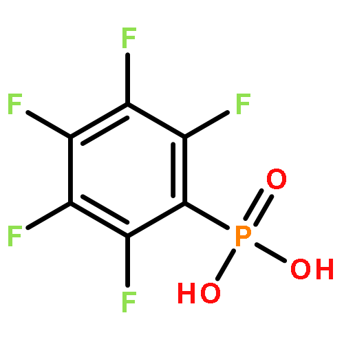
![PHOSPHONIC ACID, [(3,5-DIFLUOROPHENYL)METHYL]-, DIETHYL ESTER](http://img.cochemist.com/ccimg/451500/451455-96-2.png)
![PHOSPHONIC ACID, [(3,5-DIFLUOROPHENYL)METHYL]-, DIETHYL ESTER](http://img.cochemist.com/ccimg/451500/451455-96-2_b.png)
![2H-Thieno[3,4-b][1,4]dioxepin-3-methanol, 3,4-dihydro-3-methyl-](/data/chemimg/123200/426263-16-3.png)
![2H-Thieno[3,4-b][1,4]dioxepin-3-methanol, 3,4-dihydro-3-methyl-](/data/chemimg/123200/426263-16-3_b.png)


![2H-Thieno[3,4-b][1,4]dioxepin, 3,3-diethyl-3,4-dihydro-](/data/chemimg/123200/259139-19-0.png)
![2H-Thieno[3,4-b][1,4]dioxepin, 3,3-diethyl-3,4-dihydro-](/data/chemimg/123200/259139-19-0_b.png)


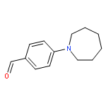
![Propanedinitrile, [[4-(hexahydro-1H-azepin-1-yl)phenyl]methylene]-](http://img.cochemist.com/ccimg/199300/199297-13-7.png)
![Propanedinitrile, [[4-(hexahydro-1H-azepin-1-yl)phenyl]methylene]-](http://img.cochemist.com/ccimg/199300/199297-13-7_b.png)
![1,2-Benzenediol, 4,5-bis[2-(phenylmethoxy)ethoxy]-](http://img.cochemist.com/ccimg/186100/186019-22-7.png)
![1,2-Benzenediol, 4,5-bis[2-(phenylmethoxy)ethoxy]-](http://img.cochemist.com/ccimg/186100/186019-22-7_b.png)


![2H-Thieno[3,4-b][1,4]dioxepin, 3,4-dihydro-](/data/chemimg/123200/155861-77-1.png)
![2H-Thieno[3,4-b][1,4]dioxepin, 3,4-dihydro-](/data/chemimg/123200/155861-77-1_b.png)


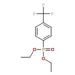
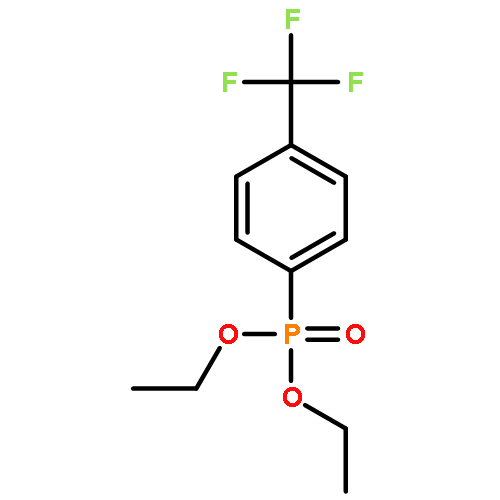
![Phosphonic acid, [[4-(trifluoromethyl)phenyl]methyl]-](http://img.cochemist.com/ccimg/146800/146780-15-6.png)
![Phosphonic acid, [[4-(trifluoromethyl)phenyl]methyl]-](http://img.cochemist.com/ccimg/146800/146780-15-6_b.png)
![Poly[2-methoxy-5-(2-ethylhexyloxy)-1,4-phenylenevinylene]](http://img.cochemist.com/ccimg/138200/138184-36-8.png)
![Poly[2-methoxy-5-(2-ethylhexyloxy)-1,4-phenylenevinylene]](http://img.cochemist.com/ccimg/138200/138184-36-8_b.png)
![Benzene, 1,3-bis[[3,5-bis[[3,5-bis(phenylmethoxy)phenyl]methoxy]phenyl]methoxy]-5-(bromomethyl)-](/data/chemimg/107700/137472-17-4.png)
![Benzene, 1,3-bis[[3,5-bis[[3,5-bis(phenylmethoxy)phenyl]methoxy]phenyl]methoxy]-5-(bromomethyl)-](/data/chemimg/107700/137472-17-4_b.png)


![37H,39H-Tetranaphtho[2,3-b:2',3'-g:2'',3''-l:2''',3'''-q]porphyrazine,5,9,14,18,23,27,32,36-octabutoxy-](/data/chemimg/114000/105528-25-4.png)
![37H,39H-Tetranaphtho[2,3-b:2',3'-g:2'',3''-l:2''',3'''-q]porphyrazine,5,9,14,18,23,27,32,36-octabutoxy-](/data/chemimg/114000/105528-25-4_b.png)
![Ethanol, 2-[[(2E)-3-phenyl-2-propenyl]oxy]-](http://img.cochemist.com/ccimg/99600/99522-43-7.png)
![Ethanol, 2-[[(2E)-3-phenyl-2-propenyl]oxy]-](http://img.cochemist.com/ccimg/99600/99522-43-7_b.png)
![Anthra[2,1,9-def:6,5,10-d'e'f']diisoquinoline-1,3,8,10(2H,9H)-tetrone,2,9-ditridecyl-](http://img.cochemist.com/ccimg/95700/95689-92-2.png)
![Anthra[2,1,9-def:6,5,10-d'e'f']diisoquinoline-1,3,8,10(2H,9H)-tetrone,2,9-ditridecyl-](http://img.cochemist.com/ccimg/95700/95689-92-2_b.png)

![1,3-DIOXOLANE, 2-[(1E)-2-PHENYLETHENYL]-](http://img.cochemist.com/ccimg/84000/83977-12-2.png)
![1,3-DIOXOLANE, 2-[(1E)-2-PHENYLETHENYL]-](http://img.cochemist.com/ccimg/84000/83977-12-2_b.png)
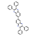
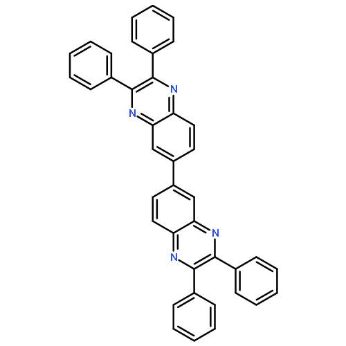
![Pyrazino[2,3-g]quinoxaline, 2,3,7,8-tetraphenyl-](http://img.cochemist.com/ccimg/80900/80829-03-4.png)
![Pyrazino[2,3-g]quinoxaline, 2,3,7,8-tetraphenyl-](http://img.cochemist.com/ccimg/80900/80829-03-4_b.png)


![[4-(piperidin-1-yl)benzylidene]propanedinitrile](http://img.cochemist.com/ccimg/66900/66883-91-8.png)
![[4-(piperidin-1-yl)benzylidene]propanedinitrile](http://img.cochemist.com/ccimg/66900/66883-91-8_b.png)
![[1,1'-BIPHENYL]-4,4'-DIAMINE, N,N'-BIS(4-METHOXYPHENYL)-](http://img.cochemist.com/ccimg/59200/59131-00-9.png)
![[1,1'-BIPHENYL]-4,4'-DIAMINE, N,N'-BIS(4-METHOXYPHENYL)-](http://img.cochemist.com/ccimg/59200/59131-00-9_b.png)


![(1,10-Phenanthroline)tris[4,4,4-trifluoro-1-(2-thienyl)-1,3-butanedionato]europium(III)](http://img.cochemist.com/ccimg/18000/17904-86-8.png)
![(1,10-Phenanthroline)tris[4,4,4-trifluoro-1-(2-thienyl)-1,3-butanedionato]europium(III)](http://img.cochemist.com/ccimg/18000/17904-86-8_b.png)


![3',6'-Dihydroxy-3H-spiro[isobenzofuran-1,9'-xanthen]-3-one](http://img.cochemist.com/ccimg/2400/2321-07-5.png)
![3',6'-Dihydroxy-3H-spiro[isobenzofuran-1,9'-xanthen]-3-one](http://img.cochemist.com/ccimg/2400/2321-07-5_b.png)


![[(3-chlorophenyl)hydrazono]malononitrile](http://img.cochemist.com/ccimg/600/555-60-2.png)
![[(3-chlorophenyl)hydrazono]malononitrile](http://img.cochemist.com/ccimg/600/555-60-2_b.png)


![2,9-Dibutylisoquinolino[4',5',6':6,5,10]anthra[2,1,9-def]isoquino line-1,3,8,10(2H,9H)-tetrone](http://img.cochemist.com/ccimg/52100/52000-75-6.png)
![2,9-Dibutylisoquinolino[4',5',6':6,5,10]anthra[2,1,9-def]isoquino line-1,3,8,10(2H,9H)-tetrone](http://img.cochemist.com/ccimg/52100/52000-75-6_b.png)


![Quino[2,3-b]acridine-7,14-dione, 5,12-dihydro-5,12-bis(3-methylbutyl)-](http://img.cochemist.com/ccimg/229100/229030-52-8.png)
![Quino[2,3-b]acridine-7,14-dione, 5,12-dihydro-5,12-bis(3-methylbutyl)-](http://img.cochemist.com/ccimg/229100/229030-52-8_b.png)
![Thieno[3,4-b]-1,4-dioxin-2-methanol, 2,3-dihydro-](/data/chemimg/519700/146796-02-3.png)
![Thieno[3,4-b]-1,4-dioxin-2-methanol, 2,3-dihydro-](/data/chemimg/519700/146796-02-3_b.png)