Co-reporter:Krishnamoorthy Thirumal, Wee Kiang Chong, Wei Xie, Rakesh Ganguly, Subas Kumar Muduli, Matthew Sherburne, Mark Asta, Subodh Mhaisalkar, Tze Chien Sum, Han Sen Soo, and Nripan Mathews
Chemistry of Materials May 9, 2017 Volume 29(Issue 9) pp:3947-3947
Publication Date(Web):April 7, 2017
DOI:10.1021/acs.chemmater.7b00073
Hybrid two-dimensional (2D) lead halide perovskites have been employed in optoelectronic applications, including white-light emission for light-emitting diodes (LEDs). However, until now, there have been limited reports about white-light-emitting lead halide perovskites with experimental insights into the mechanism of the broadband emission. Here, we present white-light emission from a 2D hybrid lead chloride perovskite, using the widely known phenethylammonium cation. The single-crystal X-ray structural data, time-resolved photophysical measurements, and density functional theory calculations are consistent with broadband emission arising from strong exciton–phonon coupling with the organic lattice, which is independent of surface defects. The phenethylammonium lead chloride material exhibits a remarkably high color rendering index of 84, a CIE coordinate of (0.37,0.42), a CCT of 4426, and photostability, making it ideal for natural white LED applications.
Co-reporter:Mohit Rameshchandra Kulkarni, Rohit Abraham John, Mayank Rajput, Naveen Tiwari, Natalia Yantara, Anh Chien Nguyen, and Nripan Mathews
ACS Applied Materials & Interfaces May 3, 2017 Volume 9(Issue 17) pp:15015-15015
Publication Date(Web):April 19, 2017
DOI:10.1021/acsami.6b16840
Electronic skins need to be versatile and able to detect multiple inputs beyond simple pressure and touch while having attributes of transparency and facile manufacturability. Herein, we demonstrate a versatile nanostructured transparent sensor capable of detecting wide range of pressures and proximity as well as novel nonoptical detection of printed patterns. The architecture and fabrication processes are straightforward and show robustness to repeated cycling and testing. The sensor displays good sensitivity and stability from 30 Pa to 5 kPa without the use of microstructuration and is conformal and sensitive to be utilized as a wrist-based heart-rate monitor. Highly sensitive proximity detection is shown from a distance of 9 cm. Finally, a unique nonoptical pattern recognition dependent on the difference in the dielectric constant between ink and paper is also demonstrated, indicating the multifunctionality of this simple architecture.Keywords: capacitive sensor; multifunctional sensor; nonoptical readout; proximity sensing; transparent pressure sensor;
Co-reporter:Yan Fong Ng, Nur Fadilah Jamaludin, Natalia Yantara, Mingjie Li, Venkata Kameshwar Rao Irukuvarjula, Hilmi Volkan Demir, Tze Chien Sum, Subodh Mhaisalkar, and Nripan Mathews
ACS Omega June 2017? Volume 2(Issue 6) pp:2757-2757
Publication Date(Web):June 19, 2017
DOI:10.1021/acsomega.7b00360
Research into perovskite-based light-emitting diodes (PeLEDs) has been rapidly gaining momentum since the initial reports of green-emitting methylammonium lead bromide (CH3NH3PbBr3)-based devices were published. However, issues pertaining to its stability and morphological control still hamper progress toward high performing devices. Solvent engineering, a technique typically employed to modulate film crystallization, offers little opportunity for scale-up due to the tendency for inhomogeneous film growth and low degree of reproducibility. Here, we propose and show a simple gas-facilitated process to deposit a stable, all-inorganic perovskite CsPbBr3 film. The formation of smaller and less percolated grains, which gives rise to enhanced optical properties, highlights the importance of spatial charge confinement in the film. Consequently, the performance of our PeLEDs shows great improvement, with luminance as high as 8218 cd m–2 and turn-on voltage as low as 2.4 V. Concomitantly, the current efficiency and EQE of our device were increased to 0.72 cd A–1 and 0.088%, respectively. High reproducibility in the performance of PeLEDs fabricated using this process opens the path for large-area devices.Topics: Diffraction; Electric properties; Electric transport processes and properties; Luminescence; Luminescence; Phase; Phase transition; Plasmonic and Photonic Structures and Devices; Quantum mechanical methods; Quantum mechanical methods; Surface structure;
Co-reporter:Cheng Sun;Minrui Zheng;Chorng Haur Sow;Lydia Helena Wong;Subodh G. Mhaisalkar
The Journal of Physical Chemistry C January 21, 2010 Volume 114(Issue 2) pp:1331-1336
Publication Date(Web):2017-2-22
DOI:10.1021/jp909673j
Highly oriented tin oxide (SnO2) nanowire network (nanonets) based devices fabricated through photolithography-free techniques are studied. These nanowire networks are studied at submillimeter scales for their utilization as the active material in thin film transistors for macroelectronics. The SnO2 nanowire network transistors show excellent device characteristics and possess electron mobilities of ∼7.5 cm2 V−1 s−1 and on/off ratios between 106 and 108 with channel lengths ranging from 75 to 175 μm. Exposure of the SnO2 nanonet transistors to the ambient results in positive threshold voltage shifts due to electron trapping by oxygen at the nanowire surface. On the contrary, the electrical properties of the devices remained unchanged upon passivation by a polystyrene (PS) layer, which demonstrates a practical way to enhance the device performance in air. These results suggest that SnO2 nanonets that offer fault tolerance, flexibility, and high transparency due to low areal coverage could be a suitable candidate for low-cost, large-area electronics.
Co-reporter:Teck Ming Koh, Junye Huang, Ishita Neogi, Pablo P. Boix, Subodh G. Mhaisalkar, and Nripan Mathews
ACS Applied Materials & Interfaces August 30, 2017 Volume 9(Issue 34) pp:28743-28743
Publication Date(Web):August 11, 2017
DOI:10.1021/acsami.7b07780
In this manuscript we reveal the formation of bilayered hybrid perovskites of a new lower dimensional perovskite family, (CHMA)2(MA)n−1PbnI3 with n = 1–5, with high ambient stability via its crystallization driven self-assembly process. The spun-coated perovskite solution tends to crystallize and undergo phase separation during annealing, resulting in the formation of 2D/3D bilayered hybrid perovskites. Remarkably, this 2D/3D hybrid perovskites possess striking moisture resistance and displays high ambient stability up to 65 days. The bilayered approach in combining 3D and 2D perovskites could lead to a new era of perovskite research for high-efficiency photovoltaics with outstanding stability, with the 3D perovskite providing excellent electronic properties while the 2D perovskite endows it moisture stability.Keywords: air stability; bilayered perovskite; mixed-dimensionality; phase separation; self-assembly;
Co-reporter:Biplab Ghosh, Sudip Chakraborty, Hao Wei, Claude Guet, Shuzhou Li, Subodh Mhaisalkar, and Nripan Mathews
The Journal of Physical Chemistry C August 17, 2017 Volume 121(Issue 32) pp:17062-17062
Publication Date(Web):July 4, 2017
DOI:10.1021/acs.jpcc.7b03501
Bismuth-based halide perovskite derivatives have now attracted huge attention for photovoltaic (PV) applications after the unparalleled success of lead-based halide perovskites. However, the performances of PV devices based on these compounds are poor, despite theoretical predictions. In this Article, we have investigated the electronic structure and defect formation energies of Cs3Bi2I9 using density functional theory (DFT) calculations. The calculated electronic bandstructure indicates an indirect bandgap and high carrier effective masses. Our calculations reveal a large stability region for this compound; however, deep level defects are quite prominent. Even the varying chemical potentials from the stoichiometric region do not eliminate the presence of deep defects, ultimately limiting photovoltaic efficiencies.
Co-reporter:Asim Guchhait, Herlina Arianita Dewi, Shin Woei Leow, Hao Wang, Guifang Han, Firdaus Bin Suhaimi, Subodh Mhaisalkar, Lydia Helena Wong, and Nripan Mathews
ACS Energy Letters April 14, 2017 Volume 2(Issue 4) pp:807-807
Publication Date(Web):March 9, 2017
DOI:10.1021/acsenergylett.7b00187
The development of high efficiency semitransparent perovskite solar cells is necessary for application in integrated photovoltaics and tandem solar cells. However, perovskite’s sensitivity to temperature and solvents impose a restriction on following processes, thus favoring physical vapor deposition for the transparent contacts. Protection may be necessary, especially for high energy sputtering and a transparent buffer layer providing good electrode adhesion and conductivity is desired. Here we evaluate Ag and MoOx buffer layers in pursuit of high efficiency tandem solar cells. The usage of thin Ag as a buffer layer demonstrated indium tin oxide (ITO) contacts that were resistant to delamination and yielded a 16.0% efficiency of semitransparent perovskite solar cell with average transparency of 12% in visible range and >50% in near-infrared. Further application in tandem with Cu(In,Ga)Se showed an overall efficiency of 20.7% in a 4-terminal (4T) configuration, exceeding the individual efficiencies of the subcells.
Co-reporter:Yan Fong Ng;Sneha A. Kulkarni;Shayani Parida;Nur Fadilah Jamaludin;Natalia Yantara;Annalisa Bruno;Cesare Soci;Subodh Mhaisalkar
Chemical Communications 2017 vol. 53(Issue 88) pp:12004-12007
Publication Date(Web):2017/11/02
DOI:10.1039/C7CC06615E
The incorporation of phenylethylammonium bromide (PEABr) into a fully inorganic CsPbBr3 perovskite framework led to the formation of mixed-dimensional perovskites, which enhanced the photoluminescence due to efficient energy funnelling and morphological improvements. With a PEABr : CsPbBr3 ratio of 0.8 : 1, PeLEDs with a current efficiency of 6.16 cd A−1 and an EQE value of 1.97% have been achieved.
Co-reporter:Subas Kumar Muduli;Eswaraiah Varrla;You Xu;Sneha Avinash Kulkarni;Ankita Katre;Sudip Chakraborty;Shi Chen;Tze Chien Sum;Rong Xu
Journal of Materials Chemistry A 2017 vol. 5(Issue 47) pp:24874-24879
Publication Date(Web):2017/12/05
DOI:10.1039/C7TA04889K
Recently, a new class of two-dimensional black phosphorus (BP) with a visible direct band gap is predicted as a potential candidate for photo-catalysis applications. Here, we present the first experimental evidence of hydrogen (H2) evolution from aqueous solution by using BP (nanosheets and nanoparticles) under visible light illumination. Our experimental results describe that liquid phase exfoliated BP nanosheets and BP nanoparticles exhibit suitable energy level alignments for electron transfer and further proton reduction reactions in the solution under visible light illumination. Density functional theory (DFT) calculations predict that the H2 evolution activity of bilayer BP is independent of edge or center positions, which is unique in BP as compared to those of other 2D materials.
Co-reporter:Subas Kumar Muduli, Eswaraiah Varrla, Sneha Avinash Kulkarni, Guifang Han, Krishnamoorthy Thirumal, Ovadia Lev, Subodh Mhaisalkar, Nripan Mathews
Journal of Power Sources 2017 Volume 371(Volume 371) pp:
Publication Date(Web):15 December 2017
DOI:10.1016/j.jpowsour.2017.10.018
•2D Black Phosphorus has been used as a hole transporter in perovskite solar cells.•Liquid phase exfoliated black phosphorus is extensively characterized.•Efficient hole injection from perovskite into black phosphorus is shown.We demonstrate for the first-time liquid exfoliated few layers of 2D Black phosphorus (BP) nanosheets as a hole transporting material (HTM) for perovskite based solar cells. The photoelectron spectroscopy in air (PESA) measurements confirm the low laying valence band level of BP nanosheets (−5.2 eV) favourable for hole injection from CH3NH3PbI3 (MAPbI3). Our results show that ∼25% improvement in power conversion efficiency (PCE) of η = 16.4% for BP nanosheets + Spiro-OMeTAD as an HTM as compared to spiro-OMeTAD (η = 13.1%). When BP nanosheets are exclusively utilised as an HTM, a PCE of η = 7.88% is noted, an improvement over the 4% PCE values observed for HTM free devices. Photoluminescence (PL) quenching of MAPbI3 and impedance measurements further confirm the charge extraction ability of BP nanosheets. The structural and optical characterization of liquid exfoliated BP nanosheets is discussed in detail with the aid of transmission electron microscopy, Raman spectroscopy, absorption spectroscopy and photo-electron spectroscopy.
Co-reporter:Teck Ming Koh, Benny Febriansyah, Nripan Mathews
Chem 2017 Volume 2, Issue 3(Volume 2, Issue 3) pp:
Publication Date(Web):9 March 2017
DOI:10.1016/j.chempr.2017.02.015
Ruddlesden-Popper halide perovskites are now viewed as a promising avenue in perovskite solar cells in terms of both stability and high power-conversion efficiencies. We provide context to the efforts of Kanatzidis and coworkers, who, in this issue of Chem, have unveiled promising developments in the higher members of the (CH3(CH2)3NH3)2(CH3NH3)n−1PbnI3n+1 series.
Co-reporter:Varun Rai, Naveen Tiwari, Mayank Rajput, Salil M. Joshi, Anh Chien Nguyen, Nripan Mathews
Electrochimica Acta 2017 Volume 255(Volume 255) pp:
Publication Date(Web):20 November 2017
DOI:10.1016/j.electacta.2017.09.088
•Scaling up of silver based reversible electrodeposited system for large area smart window applications.•Studied the role of the redox mediator in improving switching time and transparency of EC devices.•Demonstrated reversible flexible electrochromic devices (active area 2.5 × 2.5 cm2).•Through very simple patterning strategies, large area information display and decorative patterns are demonstrated and assembled over large sheet of ITO.Silver based reversible electrochromic (EC) devices which can be used for smart windows and information display are analysed to examine the factors that determine switching time, color, and scale-up. These devices demonstrate multiple colors: silver, black, magenta, yellow and dark cyan blue with switching time as low as 5 seconds. The usage of redox mediators, applied bias, in enhancing the kinetics of the color transformation while being constrained by the electrochemical window of the DMSO solvent was examined. By a judicious combination of these factors, fabrication of large-area electrochromic devices up to 77 cm2 operating at −3.0 V for formation of mirror-like reflective state (∼100% reflectance) in less than 15 seconds; and reverse switching to transparency at 0.5 V in less than 30 seconds have been realised. Devices capable of transforming into different patterns are also demonstrated with similar switching performance.Download high-res image (127KB)Download full-size image
Co-reporter:Teck Ming Koh;Vignesh Shanmugam;Johannes Schlipf;Lukas Oesinghaus;Peter Müller-Buschbaum;N. Ramakrishnan;Varghese Swamy;Pablo P. Boix;Subodh G. Mhaisalkar
Advanced Materials 2016 Volume 28( Issue 19) pp:3653-3661
Publication Date(Web):
DOI:10.1002/adma.201506141
Co-reporter:Rohit Abraham John, Nguyen Anh Chien, Sudhanshu Shukla, Naveen Tiwari, Chen Shi, Ng Geok Ing, and Nripan Mathews
Chemistry of Materials 2016 Volume 28(Issue 22) pp:8305
Publication Date(Web):October 25, 2016
DOI:10.1021/acs.chemmater.6b03499
The challenges associated with low-temperature solution-processed metal oxide network formation have hindered the realization of high-performance solution-based electronic circuitry at temperatures lower than 200 °C. Here, UV irradiation is embarked upon as a route to effectively transform the chemical precursors to semiconducting metal oxides with high electrical quality. High-performance UV-irradiated indium oxide (In2O3) and indium zinc oxide (IZO) thin film transistors with mobility greater than 30 cm2/(V s) have been obtained from nitrate-based precursors. The chemical transformation has been monitored by detailed spectroscopic studies, physical characterization, and temperature-dependent electrical transport measurements. In comparison to thermal annealing, UV annealing seems to result in higher M–O–M network formation (depicted by M–O bonds in XPS), better removal of chemical impurities (depicted by FTIR and XPS), and structural relaxation driven electron doping, transforming the oxygen vacancies to act as shallow donors (depicted by TFT characteristics, XPS, XRD, and Urbach studies). Our results provide new insight into how UV irradiation drives metal oxide network formation and passivates the subgap density of states (DOS).
Co-reporter:P. C. Harikesh, Hemant Kumar Mulmudi, Biplab Ghosh, Teck Wee Goh, Yin Ting Teng, Krishnamoorthy Thirumal, Mark Lockrey, Klaus Weber, Teck Ming Koh, Shuzhou Li, Subodh Mhaisalkar, and Nripan Mathews
Chemistry of Materials 2016 Volume 28(Issue 20) pp:7496
Publication Date(Web):September 22, 2016
DOI:10.1021/acs.chemmater.6b03310
Even though perovskite solar cells have reached 22% efficiency within a very short span, the presence of lead is a major bottleneck to its commercial application. Tin and germanium based perovskites failed to be viable replacements due to the instability of their +2 oxidation states. Antimony could be a possible replacement, forming perovskites with structure A3M2X9. However, solution processing of Cs, organic ammonium based Sb perovskites result in the formation of the dimer phase with poor charge transport properties. Here we demonstrate that Rb can template the formation of the desired layered phase irrespective of processing methodologies, enabling the demonstration of efficient lead-free perovskite solar cells.
Co-reporter:Kunwu Fu, Christopher T. Nelson, Mary Cooper Scott, Andrew Minor, Nripan Mathews and Lydia Helena Wong
Nanoscale 2016 vol. 8(Issue 7) pp:4181-4193
Publication Date(Web):19 Jan 2016
DOI:10.1039/C5NR06362K
The stunning rise of methylammonium lead iodide perovskite material as a light harvesting material in recent years has drawn much attention in the photovoltaic community. Here, we investigated in detail the uniform and void-free perovskite capping layer in the mesoscopic perovskite devices and found it to play a critical role in determining device performance and charge recombination process. Compared to the rough surface with voids of the perovskite layer, surface of the perovskite capping layer obtained from sequential deposition process is much more uniform with less void formation and distribution within the TiO2 mesoscopic scaffold is more homogeneous, leading to much improved photovoltaic parameters of the devices. The impact of void free perovskite capping layer surface on the charge recombination processes within the mesoscopic perovskite solar cells is further scrutinized via charge extraction measurement. Modulation of precursor solution concentrations in order to further improve the perovskite layer surface morphology leads to higher efficiency and lower charge recombination rates. Inhibited charge recombination in these solar cells also matches with the higher charge density and slower photovoltage decay profiles measured.
Co-reporter:Rohit Abraham John, Anh Chien Nguyen, Yuxin Chen, Sudhanshu Shukla, Shi Chen, and Nripan Mathews
ACS Applied Materials & Interfaces 2016 Volume 8(Issue 2) pp:1139
Publication Date(Web):December 23, 2015
DOI:10.1021/acsami.5b08880
Amorphous oxide semiconductors such as indium zinc tin oxide (IZTO) are considered favorites to serve as channel materials for thin film transistors (TFTs) because they combine high charge carrier mobility with high optical transmittance, allowing for the development of transparent electronics. Although the influence of relative cationic concentrations in determining the electronic properties have been studied in sputtered and PLD films, the development of printed transparent electronics hinges on such dependencies being explored for solution-processed systems. Here, we study solution-processed indium zinc tin oxide thin film transistors (TFTs) to investigate variation in their electrical properties with change in cationic composition. Charge transport mobility ranging from 0.3 to 20.3 cm2/(V s), subthreshold swing ranging from 1.2 to 8.4 V/dec, threshold voltage ranging from −50 to 5 V, and drain current on–off ratio ranging from 3 to 6 orders of magnitude were obtained by examining different compositions of the semiconductor films. Mobility was found to increase with the incorporation of large cations such as In3+ and Sn4+ due to the vast s-orbital overlap they can achieve when compared to the intercationic distance. Subthreshold swing decreased with an increase in Zn2+ concentration due to reduced interfacial state formation between the semiconductor and dielectric. The optimized transistor obtained at a compositional ratio of In/Zn/Sn = 1:1:1, exhibited a high field-effect mobility of 8.62 cm2/(V s), subthreshold swing of 1.75 V/dec, and current on–off ratio of 106. Such impressive performances reaffirm the promise of amorphous metal oxide semiconductors for printed electronics.Keywords: activation energy; indium zinc tin oxide; mobility; on−off ratio; printed electronics; thin film transistors
Co-reporter:Saikat Bhaumik, Sjoerd A. Veldhuis, Yan Fong Ng, Mingjie Li, Subas Kumar Muduli, Tze Chien Sum, Bahulayan Damodaran, Subodh Mhaisalkar and Nripan Mathews
Chemical Communications 2016 vol. 52(Issue 44) pp:7118-7121
Publication Date(Web):26 Apr 2016
DOI:10.1039/C6CC01056C
A new protocol for the synthesis of a highly stable (over 2 months under ambient conditions) solution-processed core–shell type structure of mixed methylammonium–octylammonium lead bromide perovskite nanoparticles (5–12 nm), having spherical shape, color tunability in the blue to green spectral region (438–521 nm) and a high photoluminescence quantum yield (PLQY) of up to 92% is described. The color tunability, high PLQY and stability are due to the quantum confinement imparted by the crystal engineering associated with core–shell nanoparticle formation during growth.
Co-reporter:Daniele Cortecchia, Herlina Arianita Dewi, Jun Yin, Annalisa Bruno, Shi Chen, Tom Baikie, Pablo P. Boix, Michael Grätzel, Subodh Mhaisalkar, Cesare Soci, and Nripan Mathews
Inorganic Chemistry 2016 Volume 55(Issue 3) pp:1044-1052
Publication Date(Web):January 12, 2016
DOI:10.1021/acs.inorgchem.5b01896
Despite their extremely good performance in solar cells with efficiencies approaching 20% and the emerging application for light-emitting devices, organic–inorganic lead halide perovskites suffer from high content of toxic, polluting, and bioaccumulative Pb, which may eventually hamper their commercialization. Here, we present the synthesis of two-dimensional (2D) Cu-based hybrid perovskites and study their optoelectronic properties to investigate their potential application in solar cells and light-emitting devices, providing a new environmental-friendly alternative to Pb. The series (CH3NH3)2CuClxBr4–x was studied in detail, with the role of Cl found to be essential for stabilization. By exploiting the additional Cu d–d transitions and appropriately tuning the Br/Cl ratio, which affects ligand-to-metal charge transfer transitions, the optical absorption in this series of compounds can be extended to the near-infrared for optimal spectral overlap with the solar irradiance. In situ formation of Cu+ ions was found to be responsible for the green photoluminescence of this material set. Processing conditions for integrating Cu-based perovskites into photovoltaic device architectures, as well as the factors currently limiting photovoltaic performance, are discussed: among them, we identified the combination of low absorption coefficient and heavy mass of the holes as main limitations for the solar cell efficiency. To the best of our knowledge, this is the first demonstration of the potential of 2D copper perovskite as light harvesters and lays the foundation for further development of perovskite based on transition metals as alternative lead-free materials. Appropriate molecular design will be necessary to improve the material’s properties and solar cell performance filling the gap with the state-of-the-art Pb-based perovskite devices.
Co-reporter:Wee Kiang Chong;David Giovanni;Subodh Mhaisalkar;Ramamoorthy Ramesh;Herlina Arianita Dewi;Krishnamoorthy Thirumal;Ishita Neogi;Tze Chien Sum
Science Advances 2016 Volume 2(Issue 6) pp:e1600477
Publication Date(Web):17 Jun 2016
DOI:10.1126/sciadv.1600477
A new spin on perovskites untwined: Ultrafast optical switching and tuning of spin-energy states in layered halide perovskites.
Co-reporter:Bo Wu;Kunwu Fu;Natalia Yantara;Guichuan Xing;Shuangyong Sun;Tze Chien Sum
Advanced Energy Materials 2015 Volume 5( Issue 19) pp:
Publication Date(Web):
DOI:10.1002/aenm.201500829
Organic–inorganic hybrid perovskite solar cells based on CH3NH3PbI3 have achieved great success with efficiencies exceeding 20%. However, there are increasing concerns over some reported efficiencies as the cells are susceptible to current–voltage (I–V) hysteresis effects. It is therefore essential that the origins and mechanisms of the I–V hysteresis can clearly be understood to minimize or eradicate these hysteresis effects completely for reliable quantification. Here, a detailed electro-optical study is presented that indicates the hysteresis originates from lingering processes persisting from sub-second to tens of seconds. Photocurrent transients, photoluminescence, electroluminescence, quasi-steady state photoinduced absorption processes, and X-ray diffraction in the perovskite solar cell configuration have been monitored. The slow processes originate from the structural response of the CH3NH3PbI3 upon E-field application and/or charge accumulation, possibly involving methylammonium ions rotation/displacement and lattice distortion. The charge accumulation can arise from inefficient charge transfer at the perovskite interfaces, where it plays a pivotal role in the hysteresis. These findings underpin the significance of efficient charge transfer in reducing the hysteresis effects. Further improvements of CH3NH3PbI3-based perovskite solar cells are possible through careful surface engineering of existing TiO2 or through a judicious choice of alternative interfacial layers.
Co-reporter:David Giovanni, Hong Ma, Julianto Chua, Michael Grätzel, Ramamoorthy Ramesh, Subodh Mhaisalkar, Nripan Mathews, and Tze Chien Sum
Nano Letters 2015 Volume 15(Issue 3) pp:1553-1558
Publication Date(Web):February 3, 2015
DOI:10.1021/nl5039314
Low-temperature solution-processed organic–inorganic halide perovskite CH3NH3PbI3 has demonstrated great potential for photovoltaics and light-emitting devices. Recent discoveries of long ambipolar carrier diffusion lengths and the prediction of the Rashba effect in CH3NH3PbI3, that possesses large spin–orbit coupling, also point to a novel semiconductor system with highly promising properties for spin-based applications. Through circular pump–probe measurements, we demonstrate that highly polarized electrons of total angular momentum (J) with an initial degree of polarization Pini ∼ 90% (i.e., −30% degree of electron spin polarization) can be photogenerated in perovskites. Time-resolved Faraday rotation measurements reveal photoinduced Faraday rotation as large as 10°/μm at 200 K (at wavelength λ = 750 nm) from an ultrathin 70 nm film. These spin polarized carrier populations generated within the polycrystalline perovskite films, relax via intraband carrier spin-flip through the Elliot-Yafet mechanism. Through a simple two-level model, we elucidate the electron spin relaxation lifetime to be ∼7 ps and that of the hole is ∼1 ps. Our work highlights the potential of CH3NH3PbI3 as a new candidate for ultrafast spin switches in spintronics applications.
Co-reporter: Gurudayal, Dharani Sabba, Mulmudi Hemant Kumar, Lydia Helena Wong, James Barber, Michael Grätzel, and Nripan Mathews
Nano Letters 2015 Volume 15(Issue 6) pp:3833-3839
Publication Date(Web):March 30, 2015
DOI:10.1021/acs.nanolett.5b00616
Photoelectrochemical water splitting half reactions on semiconducting photoelectrodes have received much attention but efficient overall water splitting driven by a single photoelectrode has remained elusive due to stringent electronic and thermodynamic property requirements. Utilizing a tandem configuration wherein the total photovoltage is generated by complementary optical absorption across different semiconducting electrodes is a possible pathway to unassisted overall light-induced water splitting. Because of the low photovoltages generated by conventional photovoltaic materials (e.g., Si, CIGS), such systems typically consist of triple junction design that increases the complexity due to optoelectrical trade-offs and are also not cost-effective. Here, we show that a single solution processed organic–inorganic halide perovskite (CH3NH3PbI3) solar cell in tandem with a Fe2O3 photoanode can achieve overall unassisted water splitting with a solar-to-hydrogen conversion efficiency of 2.4%. Systematic electro-optical studies were performed to investigate the performance of tandem device. It was found that the overall efficiency was limited by the hematite’s photocurrent and onset potential. To understand these limitations, we have estimated the intrinsic solar to chemical conversion efficiency of the doped and undoped Fe2O3 photoanodes. The total photopotential generated by our tandem system (1.87 V) exceeds both the thermodynamic and kinetic requirements (1.6 V), resulting in overall water splitting without the assistance of an electrical bias.
Co-reporter:Natalia Yantara, Fang Yanan, Chen Shi, Herlina Arianita Dewi, Pablo P. Boix, Subodh G. Mhaisalkar, and Nripan Mathews
Chemistry of Materials 2015 Volume 27(Issue 7) pp:2309
Publication Date(Web):February 18, 2015
DOI:10.1021/cm502710r
The effect of film morphology on the photovoltaic performances is illustrated. Pin holes free and uniform films could be formed by slowing down the crystallization rate through additional of excess CH3NH3+. Though better film coverage is obtained, the device series resistance increases as excess CH3NH3I increases. Thermogravimetric analysis confirms the presence of residual excess CH3NH3I in the final film. When chlorine is added to the CH3NH3+ rich system, CH3NH3Cl is formed and can easily sublime during annealing at 100 °C. A little trace of excess CH3NH3Cl can be detected from thermogravic analysis, and the residual chlorine atoms match with XPS reading.
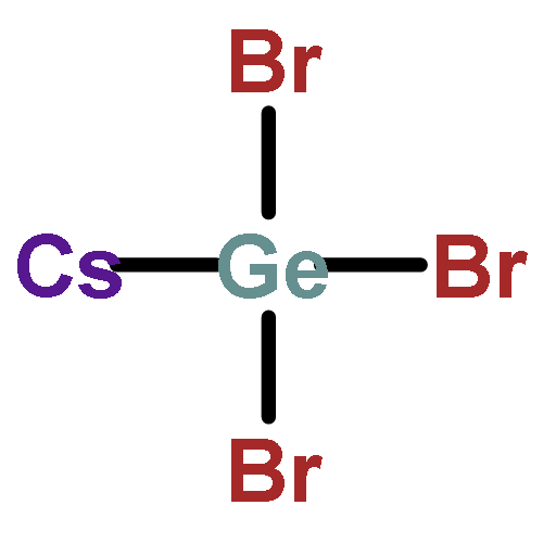
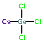
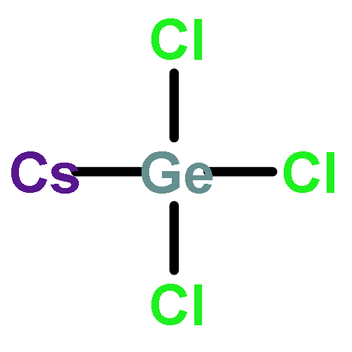
Co-reporter:Thirumal Krishnamoorthy, Hong Ding, Chen Yan, Wei Lin Leong, Tom Baikie, Ziyi Zhang, Matthew Sherburne, Shuzhou Li, Mark Asta, Nripan Mathews and Subodh G. Mhaisalkar
Journal of Materials Chemistry A 2015 vol. 3(Issue 47) pp:23829-23832
Publication Date(Web):16 Oct 2015
DOI:10.1039/C5TA05741H
Computational screening based on density-functional-theory calculations reveals Ge as a candidate element for replacing Pb in halide perovskite compounds suitable for light harvesting. Experimentally, three AGeI3 (A = Cs, CH3NH3 or HC(NH2)2) halide perovskite materials have been synthesized. These compounds are stable up to 150 °C, and have bandgaps correlated with the A-site cation size. CsGeI3-based solar cells display higher photocurrents, of about 6 mA cm−2, but are limited by poor film forming abilities and oxidising tendencies. The present results demonstrate the utility of combining computational screening and experimental efforts to develop lead-free halide perovskite compounds for photovoltaic applications.
Co-reporter:Teck Ming Koh, Thirumal Krishnamoorthy, Natalia Yantara, Chen Shi, Wei Lin Leong, Pablo P. Boix, Andrew C. Grimsdale, Subodh G. Mhaisalkar and Nripan Mathews
Journal of Materials Chemistry A 2015 vol. 3(Issue 29) pp:14996-15000
Publication Date(Web):03 Jul 2015
DOI:10.1039/C5TA00190K
A lead-free low bandgap organic–inorganic hybrid perovskite, formamidinium tin iodide, is utilized as a light absorbing layer in photovoltaics. This material has a bandgap of 1.41 eV which allows light harvesting from the near infrared region, making high photocurrents achievable. A power conversion efficiency of 2.10% was accomplished upon incorporating SnF2.
Co-reporter:Natalia Yantara, Thi Thu Trang Pham, Pablo P. Boix and Nripan Mathews
Physical Chemistry Chemical Physics 2015 vol. 17(Issue 33) pp:21694-21701
Publication Date(Web):03 Jul 2015
DOI:10.1039/C5CP02041G
The advantages of employing an interconnected periodic ZnO morphology, i.e. an inverse opal structure, in electrodeposited ZnO/Cu2O devices are presented. The solar cells are fabricated using low cost solution based methods such as spin coating and electrodeposition. The impact of inverse opal geometry, mainly the diameter and thickness, is scrutinized. By employing 3 layers of an inverse opal structure with a 300 nm pore diameter, higher short circuit photocurrents (∼84% improvement) are observed; however the open circuit voltages decrease with increasing interfacial area. Optical simulation using a finite difference time domain method shows that the inverse opal structure modulates light propagation within the devices such that more photons are absorbed close to the ZnO/Cu2O junction. This increases the collection probability resulting in improved short circuit currents.
Co-reporter:Natalia Yantara; Saikat Bhaumik; Fei Yan; Dharani Sabba; Herlina A. Dewi; Nripan Mathews; Pablo P. Boix; Hilmi Volkan Demir;Subodh Mhaisalkar
The Journal of Physical Chemistry Letters 2015 Volume 6(Issue 21) pp:4360-4364
Publication Date(Web):October 16, 2015
DOI:10.1021/acs.jpclett.5b02011
Lead-halide perovskites have transcended photovoltaics. Perovskite light-emitting diodes (PeLEDs) emerge as a new field to leverage on these fascinating semiconductors. Here, we report the first use of completely inorganic CsPbBr3 thin films for enhanced light emission through controlled modulation of the trap density by varying the CsBr-PbBr2 precursor concentration. Although pure CsPbBr3 films can be deposited from equimolar CsBr-PbBr2 and CsBr-rich solutions, strikingly narrow emission line (17 nm), accompanied by elongated radiative lifetimes (3.9 ns) and increased photoluminescence quantum yield (16%), was achieved with the latter. This is translated into the enhanced performance of the resulting PeLED devices, with lower turn-on voltage (3 V), narrow electroluminescence spectra (18 nm) and higher electroluminescence intensity (407 Cd/m2) achieved from the CsBr-rich solutions.
Co-reporter:Dharani Sabba
The Journal of Physical Chemistry C 2015 Volume 119(Issue 4) pp:1763-1767
Publication Date(Web):January 6, 2015
DOI:10.1021/jp5126624
Replacement of lead in the hybrid organic–inorganic perovskite solar cells invokes the need for non-toxic materials such as Sn. Although solution processed CsSnI3 has been demonstrated as a lead-free halide perovskite which can function as a light absorber with high photocurrent densities, the power conversion efficiencies were bottlenecked by low open circuit voltages. In this work, the open circuit voltages are modulated by chemical doping of CsSnI3 with Br leading to formation of CsSnI3-xBrx (0 ≤ x ≤ 3) perovskites. The beneficial effect of Br incorporation for Voc improvement is evident for CsSnI3 system even without the addition of SnF2. There is an evolution of the crystal structure of CsSnI3 from orthorhombic to cubic for CsSnBr3 accompanied by changes in its optical properties with a blue shift of the absorption and IPCE onset, as the Br– doping is increased. The Voc enhancement is attributed to the decrease in Sn vacancies which is reflected by the lower charge carrier densities of 1015 cm–3 and a high resistance to charge recombination in case of Br rich CsSnI3-xBrx perovskite. By the addition of SnF2 to CsSnI3-xBrx perovskite, the current densities are improved significantly.
Co-reporter:Tze Chien Sum and Nripan Mathews
Energy & Environmental Science 2014 vol. 7(Issue 8) pp:2518-2534
Publication Date(Web):02 May 2014
DOI:10.1039/C4EE00673A
Solution-processed organic–inorganic perovskite solar cells are hailed as the recent major breakthrough in low-cost photovoltaics. Power conversion efficiencies approaching those of crystalline Si solar cells (exceeding 15%) have been reported. Remarkably, such phenomenal performances were achieved in a matter of 5 years – up from ∼3.8% back in 2009. Since then, the field has expanded exponentially. In this perspective, we review the basic working mechanisms of perovskite solar cells in relation to their intrinsic properties and fundamental photophysics. The current state-of-the-art and the open questions in this maturing field are also highlighted.
Co-reporter:Mulmudi Hemant Kumar;Sabba Dharani;Wei Lin Leong;Pablo P. Boix;Rajiv Ramanujam Prabhakar;Tom Baikie;Chen Shi;Hong Ding;Ramamoorthy Ramesh;Mark Asta;Michael Graetzel;Subodh G. Mhaisalkar
Advanced Materials 2014 Volume 26( Issue 41) pp:7122-7127
Publication Date(Web):
DOI:10.1002/adma.201401991
Co-reporter:Pablo P. Boix, Kazuteru Nonomura, Nripan Mathews, Subodh G. Mhaisalkar
Materials Today 2014 Volume 17(Issue 1) pp:16-23
Publication Date(Web):January–February 2014
DOI:10.1016/j.mattod.2013.12.002
The recent emergence of efficient solar cells based on organic/inorganic lead halide perovskite absorbers promises to transform the fields of dye-sensitized, organic, and thin film solar cells. Solution processed photovoltaics incorporating perovskite absorbers have achieved efficiencies of 15% [1] in solid-state device configurations, superseding liquid dye sensitized solar cell (DSC), evaporated and tandem organic solar cells, as well as various thin film photovoltaics; thus establishing perovskite solar cells as a robust candidate for commercialization. Since the first reports in late 2012, interest has soared in the innovative device structures as well as new materials, promising further improvements. However, identifying the basic working mechanisms, which are still being debated, will be crucial to design the optimum device configuration and maximize solar cell efficiencies. Here we distill the current state-of-the-art and highlight the guidelines to ascertain the scientific challenges as well as the requisites to make this technology market-viable.
Co-reporter:Sabba Dharani, Hemant Kumar Mulmudi, Natalia Yantara, Pham Thi Thu Trang, Nam Gyu Park, Michael Graetzel, Subodh Mhaisalkar, Nripan Mathews and Pablo P. Boix
Nanoscale 2014 vol. 6(Issue 3) pp:1675-1679
Publication Date(Web):14 Oct 2013
DOI:10.1039/C3NR04857H
The good electrical and morphological characteristics of TiO2 nanofibers and the high extinction coefficient of CH3NH3PbI3 perovskite are combined to obtain a solar cell with a power conversion efficiency of 9.8%. The increase of the film thickness dramatically diminishes the performance due to the reduction in porosity of the TiO2 nanofiber framework. The optimum device (∼413 nm film thickness) is compared to a planar device, where the latter produces higher Voc but lower Jsc, and consequently lower efficiency at all measured light intensities.
Co-reporter:Thirumal Krishnamoorthy, Fu Kunwu, Pablo P. Boix, Hairong Li, Teck Ming Koh, Wei Lin Leong, Satvasheel Powar, Andrew Grimsdale, Michael Grätzel, Nripan Mathews and Subodh G. Mhaisalkar
Journal of Materials Chemistry A 2014 vol. 2(Issue 18) pp:6305-6309
Publication Date(Web):10 Feb 2014
DOI:10.1039/C4TA00486H
A novel swivel-cruciform 3,3′-bithiophene based hole-transporting material (HTM) with a low lying highest occupied molecular orbital (HOMO) level was synthesized. This new HTM (KTM3) in CH3NH3PbI3 perovskite solar cells showed a higher Voc (1.08 V) and fill factor (78.3%) compared to solar cells fabricated using the widely used spiro-OMeTAD.
Co-reporter:Cheng Sun, K. R. G. Karthik, Stevin S. Pramana, Lydia H. Wong, Jie Zhang, Huang Yizhong, Chorng Haur Sow, Nripan Mathews and Subodh G. Mhaisalkar
Journal of Materials Chemistry A 2014 vol. 2(Issue 5) pp:940-945
Publication Date(Web):15 Nov 2013
DOI:10.1039/C3TC31713G
There has been a growing interest in 1-D metal oxide semiconducting nanostructures due to their stable chemical properties and potential applications in large-area, low-cost and flexible substrates. In this current work, we used field effect transistors (FETs) built on sub-millimetre scale metal oxide nanonet to characterize the nanowire surface properties. Two variations of SnO2 nanowires, denoted as 0% O2 and 0.5% O2–Ar, were grown by changing the O2 concentration in the growth atmosphere. HR-TEM images exhibit two dissimilar surface morphologies which represent diverse surface-defect levels. While the devices showed very little semiconducting behaviour in humid air, the flow in the dry air decreased the density of free carriers dramatically. Both water vapour and oxygen were observed to contribute to the hysteresis of transfer curves. Under white light illumination, 0% O2 nanonet devices exhibited a significant photocurrent response in the controlled environment while almost no changes were observed for 0.5% O2 ones. These results confirmed the significant role of surface defects in metal-oxide nanowires and implied great potential for SnO2 nanonet FETs in the application of water gas sensors and photodetectors.
Co-reporter:Victor Bochuan Wang, Natalia Yantara, Teck Ming Koh, Staffan Kjelleberg, Qichun Zhang, Guillermo C. Bazan, Say Chye Joachim Loo and Nripan Mathews
Chemical Communications 2014 vol. 50(Issue 60) pp:8223-8226
Publication Date(Web):02 Jun 2014
DOI:10.1039/C4CC02784A
Conjugated oligoelectrolytes integrated in Escherichia coli have been proposed to act as ‘molecular wires’, inducing extracellular electron transfer. This is monitored through reduction of HAuCl4 to form gold nanoparticles. In contrast to direct electron transfer, the reduction mechanism was traced to the release of electroactive cytosolic components during oligoelectrolyte incorporation.
Co-reporter:R. Devi Chandra, Manohar Rao, Keke Zhang, Rajiv Ramanujam Prabhakar, Chen Shi, Jie Zhang, Subodh G. Mhaisalkar, and Nripan Mathews
ACS Applied Materials & Interfaces 2014 Volume 6(Issue 2) pp:773
Publication Date(Web):December 11, 2013
DOI:10.1021/am401003k
Solution processed zinc tin oxide (ZTO) thin film transistors (TFTs) were fabricated by varying the Zn/Sn composition. The addition of Sn to the zinc oxide (ZnO) films resulted in improved electrical characteristics, with devices of Zn0.7Sn0.3O composition showing the highest mobility of 7.7 cm2/(V s). An improvement in subthreshold swings was also observed, indicative of a reduction of the interfacial trap densities. Mobility studies at low temperature have been carried out, which indicated that the activation energy was reduced with Sn incorporation. Kelvin probe force microscopy was performed on the films to evaluate work function and correlated to the metal–semiconductor barrier indicating Zn0.7Sn0.3O films had the smallest barrier for charge injection. Organic–inorganic hybrid complementary inverters with a maximum gain of 10 were fabricated by integrating ZTO TFTs with poly-3-hexylthiophene (P3HT) transistors.Keywords: amorphous semiconductors; CMOS inverter; Kelvin probe; solution processing; thin film transistors; zinc tin oxide;
Co-reporter:Xinfeng Liu, Bo Wu, Qing Zhang, Jing Ngei Yip, Guannan Yu, Qihua Xiong, Nripan Mathews, and Tze Chien Sum
ACS Nano 2014 Volume 8(Issue 10) pp:10101
Publication Date(Web):September 8, 2014
DOI:10.1021/nn505020e
The origins of performance enhancement in hybrid plasmonic organic photovoltaic devices are often embroiled in a complex interaction of light scattering, localized surface plasmon resonances, exciton–plasmon energy transfer and even nonplasmonic effects. To clearly deconvolve the plasmonic contributions from a single nanostructure, we herein investigate the influence of a single silver nanowire (NW) on the charge carriers in bulk heterojunction polymer solar cells using spatially resolved optical spectroscopy, and correlate to electrical device characterization. Polarization-dependent photocurrent enhancements with a maximum of ∼36% over the reference are observed when the transverse mode of the plasmonic excitations in the Ag NW is activated. The ensuing higher absorbance and light scattering induced by the electronic motion perpendicular to the NW long axis lead to increased exciton and polaron densities instead of direct surface plasmon-exciton energy transfer. Finite-difference time-domain simulations also validate these findings. Importantly, our study at the single nanostructure level explores the fundamental limits of plasmonic enhancement achievable in organic solar cells with a single plasmonic nanostructure.Keywords: organic solar cells; performance improvement; plasmonic; silver nanowire; single nanostructure; spatially resolved spectroscopy;
Co-reporter:Zhen Li, Sneha A. Kulkarni, Pablo P. Boix, Enzheng Shi, Anyuan Cao, Kunwu Fu, Sudip K. Batabyal, Jun Zhang, Qihua Xiong, Lydia Helena Wong, Nripan Mathews, and Subodh G. Mhaisalkar
ACS Nano 2014 Volume 8(Issue 7) pp:6797
Publication Date(Web):June 13, 2014
DOI:10.1021/nn501096h
Organic–inorganic metal halide perovskite solar cells were fabricated by laminating films of a carbon nanotube (CNT) network onto a CH3NH3PbI3 substrate as a hole collector, bypassing the energy-consuming vacuum process of metal deposition. In the absence of an organic hole-transporting material and metal contact, CH3NH3PbI3 and CNTs formed a solar cell with an efficiency of up to 6.87%. The CH3NH3PbI3/CNTs solar cells were semitransparent and showed photovoltaic output with dual side illuminations due to the transparency of the CNT electrode. Adding spiro-OMeTAD to the CNT network forms a composite electrode that improved the efficiency to 9.90% due to the enhanced hole extraction and reduced recombination in solar cells. The interfacial charge transfer and transport in solar cells were investigated through photoluminescence and impedance measurements. The flexible and transparent CNT network film shows great potential for realizing flexible and semitransparent perovskite solar cells.Keywords: carbon nanotubes; hole transporter free; laminated; perovskite solar cells; vacuum-free
Co-reporter:Dr. Thi Thu Trang Pham;Teck Ming Koh;Dr. Kazuteru Nonomura; Yeng Ming Lam; Nripan Mathews; Subodh Mhaisalkar
ChemPhysChem 2014 Volume 15( Issue 6) pp:1216-1221
Publication Date(Web):
DOI:10.1002/cphc.201301056
Abstract
Mass transport has been identified as a limiting problem in the photovoltaic performance of dye-sensitized solar cells based on electrolytes consisting of ionic liquids or cobalt complexes. A mixed TiO2 macroporous–mesoporous morphology employed as photoanode is demonstrated to assist the diffusion of electrolytes with higher viscosity or consisting of bulky redox mediators, such as cobalt di-tert-butyl bipyridine [Co(dtb)3]2+/3+. This morphology with large pores improves the non-linearity of photocurrent response to light intensity indicating better diffusion. The incorporated sub-micrometer pores also reduce recombination and decrease diffusion resistance, as revealed by electrochemical impedance spectroscopy.
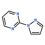
Co-reporter:Teck Ming Koh;Sabba Dharani;Dr. Hairong Li;Rajiv Ramanujam Prabhakar; Nripan Mathews; Andrew C. Grimsdale; Subodh G. Mhaisalkar
ChemSusChem 2014 Volume 7( Issue 7) pp:1909-1914
Publication Date(Web):
DOI:10.1002/cssc.201400081
Abstract
In this work, we report a new cobalt(III) complex, tris[2-(1H-pyrazol-1-yl)pyrimidine]cobalt(III) tris[bis(trifluoromethylsulfonyl)imide] (MY11), with deep redox potential (1.27 V vs NHE) as dopant for 2,2′,7,7′-tetrakis-(N,N-di-p-methoxyphenylamine)-9,9′-spirobifluorene (spiro-OMeTAD). This dopant possesses, to the best of our knowledge, the deepest redox potential among all cobalt-based dopants used in solar cell applications, allowing it to dope a wide range of hole-conductors. We demonstrate the tuning of redox potential of the Co dopant by incorporating pyrimidine moiety in the ligand. We characterize the optical and electrochemical properties of the newly synthesized dopant and show impressive spiro-to-spiro+ conversion. Lastly, we fabricate high efficiency perovskite-based solar cells using MY11 as dopant for molecular hole-conductor, spiro-OMeTAD, to reveal the impact of this dopant in photovoltaic performance. An overall power conversion efficiency of 12 % is achieved using MY11 as p-type dopant to spiro-OMeTAD.
Co-reporter:Mulmudi Hemant Kumar, Nripan Mathews, Pablo P. Boix, Kazuteru Nonomura, Satvasheel Powar, Lam Yeng Ming, Michael Graetzel and Subodh G. Mhaisalkar
Energy & Environmental Science 2013 vol. 6(Issue 11) pp:3280-3285
Publication Date(Web):23 Sep 2013
DOI:10.1039/C3EE42438C
We report a regenerative iron oxide nanorod solar cell sensitized with squarine (SQ02) dye, which improves the overall light harvesting due to the dye's complementary absorption. The use of illumination sources which enabled selective excitation of Fe2O3 and the dye independently allowed the decoupling of transport and light absorption in Fe2O3. From absorbed photon-to-current conversion efficiency (APCE) calculations, it was found out that about 80% (at λ = 680 nm) of the absorbed photons in SQ02 dye are converted to electrons and transported without any further loss into the FTO electrode. Impedance spectroscopy revealed that bulk recombination is still a prominent problem while utilizing hematite as a photoanode in a dye sensitized configuration.
Co-reporter:Mulmudi Hemant Kumar, Natalia Yantara, Sabba Dharani, Michael Graetzel, Subodh Mhaisalkar, Pablo P. Boix and Nripan Mathews
Chemical Communications 2013 vol. 49(Issue 94) pp:11089-11091
Publication Date(Web):08 Oct 2013
DOI:10.1039/C3CC46534A
A ZnO compact layer formed by electrodeposition and ZnO nanorods grown by chemical bath deposition (CBD) allow the processing of low-temperature, solution based and flexible solid state perovskite CH3NH3PbI3 solar cells. Conversion efficiencies of 8.90% were achieved on rigid substrates while the flexible ones yielded 2.62%.
Co-reporter:Guichuan Xing;Shuangyong Sun;Swee Sien Lim;Yeng Ming Lam;Michael Grätzel;Subodh Mhaisalkar;Tze Chien Sum
Science 2013 Vol 342(6156) pp:344-347
Publication Date(Web):18 Oct 2013
DOI:10.1126/science.1243167
Unrestricted Travel in Solar Cells
In the past 2 years, organolead halide perovskites have emerged as a promising class of light-harvesting media in experimental solar cells, but the physical basis for their efficiency has been unclear (see the Perspective by Hodes). Two studies now show, using a variety of time-resolved absorption and emission spectroscopic techniques, that these materials manifest relatively long diffusion paths for charge carriers energized by light absorption. Xing et al. (p. 344) independently assessed (negative) electron and (positive) hole diffusion lengths and found them well-matched to one another to the ~100-nanometer optical absorption depth. Stranks et al. (p. 341) uncovered a 10-fold greater diffusion length in a chloride-doped material, which correlates with the material's particularly efficient overall performance. Both studies highlight effective carrier diffusion as a fruitful parameter for further optimization.
Co-reporter:Rajiv Ramanujam Prabhakar, Nripan Mathews, K B Jinesh, K R G Karthik, Stevin Snellius Pramana, Binni Varghese, Chorng Haur Sow and Subodh Mhaisalkar
Journal of Materials Chemistry A 2012 vol. 22(Issue 19) pp:9678-9683
Publication Date(Web):05 Apr 2012
DOI:10.1039/C2JM16698D
Crystalline Mn doped ZnO nanowires were synthesized by chemical vapour deposition. The presence of Mn dopant was confirmed by X-Ray diffraction, Raman spectroscopy, transmission electron microscopy and X-Ray photoelectron spectroscopy. The photoconductivity of an individual Mn doped ZnO nanowire was investigated under different visible light excitations (532 and 405 nm). The nanowire exhibited high dark to photocurrent ratios (∼50), fast photocurrent response (∼100–250 ms), and reasonably high responsivity and external quantum efficiencies with good repeatability under different visible light illuminations. These results indicate that Mn doped ZnO nanowires would be promising for efficient multispectral photodetectors and optical switches.
Co-reporter:Thi Thu Trang Pham, Takeru Bessho, Nripan Mathews, Shaik M. Zakeeruddin, Yeng Ming Lam, Subodh Mhaisalkar and Michael Grätzel
Journal of Materials Chemistry A 2012 vol. 22(Issue 32) pp:16201-16204
Publication Date(Web):26 Jun 2012
DOI:10.1039/C2JM32401F
A simple cell architecture that achieves enhanced light harvesting with less dye quantity while simultaneously improving the power conversion efficiency (PCE) of dye-sensitized solar cells is presented. Polystyrene (PS) spheres of sub-micrometer size were incorporated into the titanium dioxide paste resulting in photoanodes with bimodal pore size distribution. Scanning electron micrographs of TiO2 films revealed a mixture of mesoporous and macroporous morphology in which sub-micrometer cavities created by the combustion of PS increased the light scattering, enhancing the optical path length and hence the harvesting of photons by the sensitizer. The amount of dye uptake by these films is lower than that of standard films because the high porosity reduces the total surface area. Even with lower dye adsorption, the photovoltaic performance has been maintained and even improved, mainly due to better open circuit voltage and higher fill factor. Overall, better light harvesting has helped to maintain the efficiency of dye-sensitized solar cells while saving up to 30% of dye loading and replacing the conventional 400 nm scattering layer with voids. By employing these photoanodes, an efficiency of 6.9% was achieved in ionic liquid based dye sensitized solar cells.
Co-reporter:Verawati Tjoa, Julianto Chua, Stevin S. Pramana, Jun Wei, Subodh G. Mhaisalkar, and Nripan Mathews
ACS Applied Materials & Interfaces 2012 Volume 4(Issue 7) pp:3447
Publication Date(Web):May 30, 2012
DOI:10.1021/am300437g
A low temperature route to synthesize graphene oxide–Pt nanoparticle hybrid composite by light assisted spontaneous coreduction of graphene oxide and chloroplatinic acid without reducing agent is demonstrated. Analysis indicates the importance of light as energy provider and ethanol as hole scavenger in the formation of small Pt nanoparticles (∼3 nm) on graphene oxide as well as graphene oxide reduction. Spray coating was used to deposit the hybrid material as a counter electrode in dye sensitized solar cells (DSCs). An efficiency of 6.77% for the hybrid graphene counter electrode has been obtained, higher than the control device made by low temperature sputtered Pt as counter electrode. Compatibility of the hybrid material with flexible plastic substrates was demonstrated yielding DSCs of an efficiency of 4.05%.Keywords: dye sensitized solar cells; graphene; graphene oxide; metal nanoparticle; platinum;
Co-reporter:Mrunal A. Khaderbad, Verawati Tjoa, Manohar Rao, Rohit Phandripande, Sheri Madhu, Jun Wei, Mangalampalli Ravikanth, Nripan Mathews, Subodh G. Mhaisalkar, and V. Ramgopal Rao
ACS Applied Materials & Interfaces 2012 Volume 4(Issue 3) pp:1434
Publication Date(Web):February 14, 2012
DOI:10.1021/am201691s
We report a unipolar operation in reduced graphene oxide (RGO) field-effect transistors (FETs) via modification of the source/drain (S/D) electrode interfaces with self-assembled monolayers (SAMs) of 5-(4-hydroxyphenyl)-10,15,20-tri-(p-tolyl) zinc(II) porphyrin (Zn(II)TTPOH) molecules. The dipolar Zn(II)TTPOH molecules at the RGO/platinum (Pt) S/D interface results in an increase of the electron injection barrier and a reduction of the hole-injection barrier. Using dipole measurements from Kelvin probe force microscopy and highest occupied molecular orbital–lowest unoccupied molecular orbital (HOMO–LUMO) calculations from cyclic voltammetry, the electron and hole injection barriers were calculated to be 2.2 and 0.11 eV, respectively, indicating a higher barrier for electrons, compared to that of holes. A reduced gate modulation in the electron accumulation regime in RGO devices with SAM shows that unipolar RGO FETs can be attained using a low-cost, solution-processable fabrication technique.Keywords: graphene; injection barrier; self-assembled monolayer; transistor; unipolar;
Co-reporter:Natalia Yantara, Nripan Mathews, K.B. Jinesh, Hemant Kumar Mulmudi, S.G. Mhaisalkar
Electrochimica Acta 2012 Volume 85() pp:486-491
Publication Date(Web):15 December 2012
DOI:10.1016/j.electacta.2012.08.015
The benefits and drawbacks of nanostructuring in all oxide ZnO/Cu2O solar cells were studied. The solar cells were fabricated on fluorine doped tin oxide substrates, with solution processed deposition methods. Both planar ZnO layer and Cu2O were deposited by electrodeposition while ZnO nanorods were grown by chemical bath deposition technique. It is shown that short circuit current (Jsc) of the devices increases with nanostructuring of ZnO due to electrical and optical gains. Despite improving the photocurrent, nanostructuring decreases the Voc of the device due to carrier recombination. The introduction of a thin TiO2 interfacial layer through atomic layer deposition was able to reduce the recombination.
Co-reporter:Than Zaw Oo, R. Devi Chandra, Natalia Yantara, Rajiv Ramanujam Prabhakar, Lydia H. Wong, Nripan Mathews, Subodh G. Mhaisalkar
Organic Electronics 2012 Volume 13(Issue 5) pp:870-874
Publication Date(Web):May 2012
DOI:10.1016/j.orgel.2012.01.011
Solution processed, high electron mobility and highly transparent Zinc Tin Oxide (ZTO) was successfully exploited as electron transporting buffer layer in an inverted organic solar cell. The device configuration of FTO/ZTO/P3HT:PCBM/WO3/Ag was employed. For comparison, an identical device using a sol–gel derived TiOx electron extracting layer was also fabricated. Increased short-circuit density (Jsc) and open-circuit voltage (Voc) were generated in the devices with ZTO layer in comparison to the ones with TiOx layer. It is attributed to a better electron transporting, hole blocking capacities and reduced recombination probabilities at electron collecting electrode with ZTO layer. A power conversion efficiency of 3.05% was achieved with ZTO devices.Graphical abstractHighlights► We introduce Zinc Tin Oxide (ZTO) as electron transporting layer in organic solar cell. ► Solution processed ZTO displays high electron mobility with excellent optical transparency. ► A comparative study of ZTO and TiOx buffer layers in inverted solar cells was performed. ► An efficiency of 3.05% was achieved for ZTO compared to 2.71% for TiOx.
Co-reporter:Mrunal A. Khaderbad, Verawati Tjoa, Than Z. Oo, Jun Wei, Madhu Sheri, Ravikanth Mangalampalli, V. Ramgopal Rao, Subodh G. Mhaisalkar and Nripan Mathews
RSC Advances 2012 vol. 2(Issue 10) pp:4120-4124
Publication Date(Web):19 Mar 2012
DOI:10.1039/C2RA00792D
Solution processed graphene oxide (GO) sheets are electronically insulating and are generally reduced by chemical treatment or heat treatment in a reducing environment to recover their electronic properties, forming reduced graphene oxide (rGO). Here, GO sheets were photocatalytically reduced using 5-(4-hydroxyphenyl)-10,15,20-tri(p-tolyl) zinc(II) porphyrin (Zn(II)TTPOH) under ambient conditions. After illumination in the presence of a hole scavenger and Zn(II)TTPOH, the formation of rGO was confirmed through optical absorption measurements and monitoring of the D/G peak ratios from Raman measurements. The resultant rGO formed stable aqueous suspensions with the Zn(II)TTPOH. The electron transfer from photoexcited porphyrin to GO was studied through photoluminescence measurements. Utilising this photoreduction process as a post processing strategy, an increase in conductivity and an ambipolar field effect transistor (FET) behaviour were demonstrated on prepatterned GO devices. We have also confirmed the photoreduction process at low energy wavelengths (588 nm), indicating the versatility of using metalloporphyrins as photocatalysts for graphene oxide reduction.
Co-reporter:Than Z. Oo, Nripan Mathews, Guichuan Xing, Bo Wu, Bengang Xing, Lydia H. Wong, Tze Chien Sum, and Subodh G. Mhaisalkar
The Journal of Physical Chemistry C 2012 Volume 116(Issue 10) pp:6453-6458
Publication Date(Web):February 14, 2012
DOI:10.1021/jp2099637
Solution-processed ultrafine gold nanowires (Au-NWs) have been exploited as plasmonic antennae in organic P3HT:PCBM photovoltaic cells. The careful reduction of the spacer layer thickness which allows the evanescent field to be extended into the photoactive layer and the geometry of the Au-NWs bands which favors the enhanced scattering collectively result in an increased short-circuit current density by 23.2%. The exact nature of the plasmonic effect in Au-NWs incorporated P3HT system and the critical role played by the spacer layer were studied through optical and time-resolved photoluminescence spectroscopy. The improved photocurrent in the Au-NWs integrated devices is due to an enhanced absorption in the photoactive layer which is contributed from an increased plasmon excitation field and far-field scattering of Au-NWs.
Co-reporter:Wei Lin Leong, Nripan Mathews, Bertha Tan, Subramanian Vaidyanathan, Florian Dötz and Subodh Mhaisalkar
Journal of Materials Chemistry A 2011 vol. 21(Issue 14) pp:5203-5214
Publication Date(Web):14 Feb 2011
DOI:10.1039/C0JM03974H
The implementation of plastic electronic solutions to large area displays, disposable sensor arrays, radio-frequency identification tags (RFIDs), and various smart packaging devices necessitate the development of organic memories that are solution-processable and readily integrated with the transistors for digital logic. This article highlights recent research progress made towards organic memory transistors based on charge trapping and focuses on the principles and materials (namely, nanoparticles and polymer electrets) for these devices. The challenges and prospects of charge trapping memories are also discussed.
Co-reporter:Wei Lin Leong, Nripan Mathews, Bertha Tan, Subramanian Vaidyanathan, Florian Dötz and Subodh Mhaisalkar
Journal of Materials Chemistry A 2011 vol. 21(Issue 25) pp:8971-8974
Publication Date(Web):24 May 2011
DOI:10.1039/C1JM10966A
This communication describes development of a top gate solution processable organic memory solution. Transistor memories (p-type and ambipolar) operating at voltages between 20 and 30 V with memory on–off ratios close to 103 at programming speeds of 1 ms were fabricated on glass and flexible PET substrates. Successful retention of the stored state for 1 week is also demonstrated.
Co-reporter:Verawati Tjoa, Wei Jun, Vinayak Dravid, Subodh Mhaisalkar and Nripan Mathews
Journal of Materials Chemistry A 2011 vol. 21(Issue 39) pp:15593-15599
Publication Date(Web):25 Aug 2011
DOI:10.1039/C1JM12676H
Electrical properties of reduced graphene oxide (rGO) decorated with gold and silver nanoparticles were studied. Metal nanoparticles p-dope rGO through charge transfer which causes a potential drop at the metal nanoparticle–graphene interface. Probing by reactive gases showed that the nanoparticles provide interaction sites, inducing the sensitivity to H2S and improving the sensitivity to NO2.
Co-reporter:H.K. Mulmudi, N. Mathews, X.C. Dou, L.F. Xi, S.S. Pramana, Y.M. Lam, S.G. Mhaisalkar
Electrochemistry Communications 2011 Volume 13(Issue 9) pp:951-954
Publication Date(Web):September 2011
DOI:10.1016/j.elecom.2011.06.008
Hematite nanorods were grown on fluorine doped tin oxide (FTO) substrates by hydrothermal means utilizing urea as a pH regulating agent. XRD for nanorods revealed pure hematite phase after annealing at 500 °C for 30 min with preferential orientation in the [110] direction. Electrochemical impedance spectroscopy was carried out to investigate the electrical properties. Using Mott–Schottky analysis, charge carrier density was estimated to be 5.62 × 1019 cm− 3 in the hematite nanorod array. Among the nanostructures, the n-type hematite nanorod array showed the best conversion efficiency among the samples studied in a two electrode photoelectrochemical cell. Photocurrent measurements versus light intensity were performed to investigate the device performance and the limiting factors to the performance were attributed to the short diffusion length of minority charge carriers.Highlights► We have demonstrated the growth of n-type hematite nanorods with a preferred orientation in [110] direction by hydrothermal means. ► The preferential orientation of the aligned nanorods is a step towards solving the drawback of poor electrical transport in hematite. ► Electrochemical characterization and Photoelectrochemical solar cells were fabricated.
Co-reporter:Julianto Chua, Nripan Mathews, James R. Jennings, Guangwu Yang, Qing Wang and Subodh G. Mhaisalkar
Physical Chemistry Chemical Physics 2011 vol. 13(Issue 43) pp:19314-19317
Publication Date(Web):11 Oct 2011
DOI:10.1039/C1CP22944C
We describe the application of 3-dimensional metal grid electrodes (3D-MGEs) as electron collectors in dye-sensitized solar cells (DSCs) as a replacement for fluorinated tin oxide (FTO) electrodes. Requirements, structure, advantages, and limitations of the metal grid electrodes are discussed. Solar conversion efficiencies of 6.2% have been achieved in 3D-MGE based solar cells, comparable to that fabricated on FTO (7.1%). The charge transport properties and collection efficiencies in these novel solar cells have been studied using electrochemical impedance spectroscopy.
Co-reporter:Mahshid Ahmadi, Nopphawan Phonthammachai, Tan Huei Shuan, Timothy J. White, Nripan Mathews, Subodh G. Mhaisalkar
Organic Electronics 2010 Volume 11(Issue 10) pp:1660-1667
Publication Date(Web):October 2010
DOI:10.1016/j.orgel.2010.07.007
The need for low operating voltages in organic field effect transistors (OFETs) is a motivation for the development of low temperature solution processable synthesis of high dielectric constant materials. Specifically, the glycothermal synthesis of barium titanate nanoparticles (size 10–15 nm) is described here. The effect of reaction time, temperature and reactant ratio has been studied. An 85% yield of pure BaTiO3 was obtained at a temperature of 220 °C and a reaction time of 16 h with the H2O:propanol molar ratio fixed at 1:1. A suspension of these nanoparticles in ethanol was then used to fabricate the dielectric layers in OFETs. The roughness of the spun coated layers limited the performance of these transistors. The deposition of an overlayer of sol–gel silica on the nanoparticle films improved the charge transport properties within the pentacene organic thin films by up to two orders of magnitude. The combination of solution processable high dielectric constant BaTiO3 nanoparticle layer and sol–gel silica is promising for low voltage organic electronics.
Co-reporter:T.Z. Oo, N. Mathews, T.L. Tam, G.C. Xing, T.C. Sum, A. Sellinger, L.H. Wong, S.G. Mhaisalkar
Thin Solid Films 2010 Volume 518(Issue 18) pp:5292-5299
Publication Date(Web):1 July 2010
DOI:10.1016/j.tsf.2010.04.115
Two cyano oligo-phenylene-vinylenes [α-CNOPV and β-CNOPV] distinguished by the position of cyano (CN) group at the vinylic double bond were synthesized. The acceptor oligomer CNOPVs were blended with poly(2-methoxy-5-(2′-ethyl-hexyloxy)-p-phenylenevinylene) MEH-PPV to achieve α and β blends. The pronounced influence of cyano position on the photophysical and morphological properties of blends was observed through UV–vis absorption, photoluminescence and atomic force microscopy. The optical characterization suggests wider spectral photon harvesting in α blends and more planar conformation of molecules in β blends. The steady-state and time-resolved photoluminescence study provides evidence for efficient energy transfer from α-CNOPV to MEH-PPV. On the other hand, the 3:1 β blend exhibits quenching of PL intensity indicative of charge transfer. In addition, the feasibility of MEH-PPV:CNOPV blends in organic photovoltaic devices have been investigated. The initial device parameters show that power conversion efficiency is as high as 0.05% in β 1:1 devices. The photovoltaic efficiencies were limited by weak exciton dissociation in α blends while poor morphology restricted the efficiency in β blends.
Co-reporter:Swee Sien Lim, Wee Kiang Chong, Ankur Solanki, Herlina Arianita Dewi, Subodh Mhaisalkar, Nripan Mathews and Tze Chien Sum
Physical Chemistry Chemical Physics 2016 - vol. 18(Issue 39) pp:NaN27123-27123
Publication Date(Web):2016/06/13
DOI:10.1039/C6CP02640K
Precise morphological control in perovskite films is key to high performance photovoltaic and light emitting devices. However, a clear understanding of the interplay of morphological effects from substrate/perovskite antisolvent treatments on the charge dynamics is still severely lacking. Through detailed ultrafast optical spectroscopy, we correlate the morphology-kinetics relationship in a combination of substrate/film treated samples (i.e., plasma-cleaned vs. piranha-etched substrates and solvent (toluene)-engineered (or toluene anti-solvent treated) perovskite films). Our findings reveal that toluene-dripped treatment has a more pronounced influence on the morphology of perovskite films prepared on plasma-cleaned substrates over those on piranha-etched substrates. Surprisingly, the highly effective toluene-dripping/washing approach reported in the literature increases the surface trap densities of perovskite films. Despite the marked improvements in the surface morphology of the toluene-dripped films, there is only a slight improvement in the carrier relaxation lifetimes – likely due to the competition between the morphology improvements and the increased surface trap densities. In addition, the injection of photoexcited holes to spiro-OMeTAD from toluene-dripped films on piranha-etched substrates is inhibited, possibly due to a realignment of the energy bands. Nonetheless, piranha-etching of the substrates could possibly offer an approach to improve the balance between the electron and hole diffusion lengths in the perovskite film. Importantly, our findings would help unravel the complex relationship of substrate/film treatments on the morphology and charge kinetics in perovskite thin films.
Co-reporter:Saikat Bhaumik, Sjoerd A. Veldhuis, Yan Fong Ng, Mingjie Li, Subas Kumar Muduli, Tze Chien Sum, Bahulayan Damodaran, Subodh Mhaisalkar and Nripan Mathews
Chemical Communications 2016 - vol. 52(Issue 44) pp:NaN7121-7121
Publication Date(Web):2016/04/26
DOI:10.1039/C6CC01056C
A new protocol for the synthesis of a highly stable (over 2 months under ambient conditions) solution-processed core–shell type structure of mixed methylammonium–octylammonium lead bromide perovskite nanoparticles (5–12 nm), having spherical shape, color tunability in the blue to green spectral region (438–521 nm) and a high photoluminescence quantum yield (PLQY) of up to 92% is described. The color tunability, high PLQY and stability are due to the quantum confinement imparted by the crystal engineering associated with core–shell nanoparticle formation during growth.
Co-reporter:Victor Bochuan Wang, Natalia Yantara, Teck Ming Koh, Staffan Kjelleberg, Qichun Zhang, Guillermo C. Bazan, Say Chye Joachim Loo and Nripan Mathews
Chemical Communications 2014 - vol. 50(Issue 60) pp:NaN8226-8226
Publication Date(Web):2014/06/02
DOI:10.1039/C4CC02784A
Conjugated oligoelectrolytes integrated in Escherichia coli have been proposed to act as ‘molecular wires’, inducing extracellular electron transfer. This is monitored through reduction of HAuCl4 to form gold nanoparticles. In contrast to direct electron transfer, the reduction mechanism was traced to the release of electroactive cytosolic components during oligoelectrolyte incorporation.
Co-reporter:Mulmudi Hemant Kumar, Natalia Yantara, Sabba Dharani, Michael Graetzel, Subodh Mhaisalkar, Pablo P. Boix and Nripan Mathews
Chemical Communications 2013 - vol. 49(Issue 94) pp:NaN11091-11091
Publication Date(Web):2013/10/08
DOI:10.1039/C3CC46534A
A ZnO compact layer formed by electrodeposition and ZnO nanorods grown by chemical bath deposition (CBD) allow the processing of low-temperature, solution based and flexible solid state perovskite CH3NH3PbI3 solar cells. Conversion efficiencies of 8.90% were achieved on rigid substrates while the flexible ones yielded 2.62%.
Co-reporter:Teck Ming Koh, Thirumal Krishnamoorthy, Natalia Yantara, Chen Shi, Wei Lin Leong, Pablo P. Boix, Andrew C. Grimsdale, Subodh G. Mhaisalkar and Nripan Mathews
Journal of Materials Chemistry A 2015 - vol. 3(Issue 29) pp:NaN15000-15000
Publication Date(Web):2015/07/03
DOI:10.1039/C5TA00190K
A lead-free low bandgap organic–inorganic hybrid perovskite, formamidinium tin iodide, is utilized as a light absorbing layer in photovoltaics. This material has a bandgap of 1.41 eV which allows light harvesting from the near infrared region, making high photocurrents achievable. A power conversion efficiency of 2.10% was accomplished upon incorporating SnF2.
Co-reporter:Thirumal Krishnamoorthy, Fu Kunwu, Pablo P. Boix, Hairong Li, Teck Ming Koh, Wei Lin Leong, Satvasheel Powar, Andrew Grimsdale, Michael Grätzel, Nripan Mathews and Subodh G. Mhaisalkar
Journal of Materials Chemistry A 2014 - vol. 2(Issue 18) pp:NaN6309-6309
Publication Date(Web):2014/02/10
DOI:10.1039/C4TA00486H
A novel swivel-cruciform 3,3′-bithiophene based hole-transporting material (HTM) with a low lying highest occupied molecular orbital (HOMO) level was synthesized. This new HTM (KTM3) in CH3NH3PbI3 perovskite solar cells showed a higher Voc (1.08 V) and fill factor (78.3%) compared to solar cells fabricated using the widely used spiro-OMeTAD.
Co-reporter:Thirumal Krishnamoorthy, Hong Ding, Chen Yan, Wei Lin Leong, Tom Baikie, Ziyi Zhang, Matthew Sherburne, Shuzhou Li, Mark Asta, Nripan Mathews and Subodh G. Mhaisalkar
Journal of Materials Chemistry A 2015 - vol. 3(Issue 47) pp:NaN23832-23832
Publication Date(Web):2015/10/16
DOI:10.1039/C5TA05741H
Computational screening based on density-functional-theory calculations reveals Ge as a candidate element for replacing Pb in halide perovskite compounds suitable for light harvesting. Experimentally, three AGeI3 (A = Cs, CH3NH3 or HC(NH2)2) halide perovskite materials have been synthesized. These compounds are stable up to 150 °C, and have bandgaps correlated with the A-site cation size. CsGeI3-based solar cells display higher photocurrents, of about 6 mA cm−2, but are limited by poor film forming abilities and oxidising tendencies. The present results demonstrate the utility of combining computational screening and experimental efforts to develop lead-free halide perovskite compounds for photovoltaic applications.
Co-reporter:Cheng Sun, K. R. G. Karthik, Stevin S. Pramana, Lydia H. Wong, Jie Zhang, Huang Yizhong, Chorng Haur Sow, Nripan Mathews and Subodh G. Mhaisalkar
Journal of Materials Chemistry A 2014 - vol. 2(Issue 5) pp:NaN945-945
Publication Date(Web):2013/11/15
DOI:10.1039/C3TC31713G
There has been a growing interest in 1-D metal oxide semiconducting nanostructures due to their stable chemical properties and potential applications in large-area, low-cost and flexible substrates. In this current work, we used field effect transistors (FETs) built on sub-millimetre scale metal oxide nanonet to characterize the nanowire surface properties. Two variations of SnO2 nanowires, denoted as 0% O2 and 0.5% O2–Ar, were grown by changing the O2 concentration in the growth atmosphere. HR-TEM images exhibit two dissimilar surface morphologies which represent diverse surface-defect levels. While the devices showed very little semiconducting behaviour in humid air, the flow in the dry air decreased the density of free carriers dramatically. Both water vapour and oxygen were observed to contribute to the hysteresis of transfer curves. Under white light illumination, 0% O2 nanonet devices exhibited a significant photocurrent response in the controlled environment while almost no changes were observed for 0.5% O2 ones. These results confirmed the significant role of surface defects in metal-oxide nanowires and implied great potential for SnO2 nanonet FETs in the application of water gas sensors and photodetectors.
Co-reporter:Rajiv Ramanujam Prabhakar, Nripan Mathews, K B Jinesh, K R G Karthik, Stevin Snellius Pramana, Binni Varghese, Chorng Haur Sow and Subodh Mhaisalkar
Journal of Materials Chemistry A 2012 - vol. 22(Issue 19) pp:NaN9683-9683
Publication Date(Web):2012/04/05
DOI:10.1039/C2JM16698D
Crystalline Mn doped ZnO nanowires were synthesized by chemical vapour deposition. The presence of Mn dopant was confirmed by X-Ray diffraction, Raman spectroscopy, transmission electron microscopy and X-Ray photoelectron spectroscopy. The photoconductivity of an individual Mn doped ZnO nanowire was investigated under different visible light excitations (532 and 405 nm). The nanowire exhibited high dark to photocurrent ratios (∼50), fast photocurrent response (∼100–250 ms), and reasonably high responsivity and external quantum efficiencies with good repeatability under different visible light illuminations. These results indicate that Mn doped ZnO nanowires would be promising for efficient multispectral photodetectors and optical switches.
Co-reporter:Thi Thu Trang Pham, Takeru Bessho, Nripan Mathews, Shaik M. Zakeeruddin, Yeng Ming Lam, Subodh Mhaisalkar and Michael Grätzel
Journal of Materials Chemistry A 2012 - vol. 22(Issue 32) pp:NaN16204-16204
Publication Date(Web):2012/06/26
DOI:10.1039/C2JM32401F
A simple cell architecture that achieves enhanced light harvesting with less dye quantity while simultaneously improving the power conversion efficiency (PCE) of dye-sensitized solar cells is presented. Polystyrene (PS) spheres of sub-micrometer size were incorporated into the titanium dioxide paste resulting in photoanodes with bimodal pore size distribution. Scanning electron micrographs of TiO2 films revealed a mixture of mesoporous and macroporous morphology in which sub-micrometer cavities created by the combustion of PS increased the light scattering, enhancing the optical path length and hence the harvesting of photons by the sensitizer. The amount of dye uptake by these films is lower than that of standard films because the high porosity reduces the total surface area. Even with lower dye adsorption, the photovoltaic performance has been maintained and even improved, mainly due to better open circuit voltage and higher fill factor. Overall, better light harvesting has helped to maintain the efficiency of dye-sensitized solar cells while saving up to 30% of dye loading and replacing the conventional 400 nm scattering layer with voids. By employing these photoanodes, an efficiency of 6.9% was achieved in ionic liquid based dye sensitized solar cells.
Co-reporter:Wei Lin Leong, Nripan Mathews, Bertha Tan, Subramanian Vaidyanathan, Florian Dötz and Subodh Mhaisalkar
Journal of Materials Chemistry A 2011 - vol. 21(Issue 14) pp:NaN5214-5214
Publication Date(Web):2011/02/14
DOI:10.1039/C0JM03974H
The implementation of plastic electronic solutions to large area displays, disposable sensor arrays, radio-frequency identification tags (RFIDs), and various smart packaging devices necessitate the development of organic memories that are solution-processable and readily integrated with the transistors for digital logic. This article highlights recent research progress made towards organic memory transistors based on charge trapping and focuses on the principles and materials (namely, nanoparticles and polymer electrets) for these devices. The challenges and prospects of charge trapping memories are also discussed.
Co-reporter:Wei Lin Leong, Nripan Mathews, Bertha Tan, Subramanian Vaidyanathan, Florian Dötz and Subodh Mhaisalkar
Journal of Materials Chemistry A 2011 - vol. 21(Issue 25) pp:NaN8974-8974
Publication Date(Web):2011/05/24
DOI:10.1039/C1JM10966A
This communication describes development of a top gate solution processable organic memory solution. Transistor memories (p-type and ambipolar) operating at voltages between 20 and 30 V with memory on–off ratios close to 103 at programming speeds of 1 ms were fabricated on glass and flexible PET substrates. Successful retention of the stored state for 1 week is also demonstrated.
Co-reporter:Verawati Tjoa, Wei Jun, Vinayak Dravid, Subodh Mhaisalkar and Nripan Mathews
Journal of Materials Chemistry A 2011 - vol. 21(Issue 39) pp:NaN15599-15599
Publication Date(Web):2011/08/25
DOI:10.1039/C1JM12676H
Electrical properties of reduced graphene oxide (rGO) decorated with gold and silver nanoparticles were studied. Metal nanoparticles p-dope rGO through charge transfer which causes a potential drop at the metal nanoparticle–graphene interface. Probing by reactive gases showed that the nanoparticles provide interaction sites, inducing the sensitivity to H2S and improving the sensitivity to NO2.
Co-reporter:Natalia Yantara, Thi Thu Trang Pham, Pablo P. Boix and Nripan Mathews
Physical Chemistry Chemical Physics 2015 - vol. 17(Issue 33) pp:NaN21701-21701
Publication Date(Web):2015/07/03
DOI:10.1039/C5CP02041G
The advantages of employing an interconnected periodic ZnO morphology, i.e. an inverse opal structure, in electrodeposited ZnO/Cu2O devices are presented. The solar cells are fabricated using low cost solution based methods such as spin coating and electrodeposition. The impact of inverse opal geometry, mainly the diameter and thickness, is scrutinized. By employing 3 layers of an inverse opal structure with a 300 nm pore diameter, higher short circuit photocurrents (∼84% improvement) are observed; however the open circuit voltages decrease with increasing interfacial area. Optical simulation using a finite difference time domain method shows that the inverse opal structure modulates light propagation within the devices such that more photons are absorbed close to the ZnO/Cu2O junction. This increases the collection probability resulting in improved short circuit currents.
Co-reporter:Julianto Chua, Nripan Mathews, James R. Jennings, Guangwu Yang, Qing Wang and Subodh G. Mhaisalkar
Physical Chemistry Chemical Physics 2011 - vol. 13(Issue 43) pp:NaN19317-19317
Publication Date(Web):2011/10/11
DOI:10.1039/C1CP22944C
We describe the application of 3-dimensional metal grid electrodes (3D-MGEs) as electron collectors in dye-sensitized solar cells (DSCs) as a replacement for fluorinated tin oxide (FTO) electrodes. Requirements, structure, advantages, and limitations of the metal grid electrodes are discussed. Solar conversion efficiencies of 6.2% have been achieved in 3D-MGE based solar cells, comparable to that fabricated on FTO (7.1%). The charge transport properties and collection efficiencies in these novel solar cells have been studied using electrochemical impedance spectroscopy.