Co-reporter:Hye Jin Cho, Seok-Ju Kang, Sang Myeon Lee, Mingyu Jeong, Gyoungsik Kim, Yong-Young Noh, and Changduk Yang
ACS Applied Materials & Interfaces September 13, 2017 Volume 9(Issue 36) pp:30755-30755
Publication Date(Web):August 21, 2017
DOI:10.1021/acsami.7b07856
To simultaneously assess the impact of molecular weight (Mn) and alkyl substituent variations of polymers on the structural and optoelectronic properties, herein, we conduct a systematic study of a series of poly(thienoisoindigo-alt-naphthalene) (PTIIG-Np)-based polymers containing different alkyl substituents (2-hexyldecyl (HD), 2-octyldodecyl (OD), and 2-decyltetradecyl (DT) chains) and Mn’s (low (L) and high (H)). All of the polymers produce almost identical energy levels, whereas their optical spectra show a clear dependence on Mn’s and the alkyl substituents. Interestingly, increasing the alkyl substituent sizes of the polymers steadily increases the lamellar d-spacings (d100), ultimately leading to a densely packed lamellar structure for PTIIGHD-Np. In addition, both H-PTIIGOD-Np and H-PTIIGDT-Np exhibit larger π-stacking crystallites than the corresponding low-Mn polymers, while for PTIIGHD-Np, their size increases in the low-Mn batch. Ultimately, L-PTIIGHD-Np shows the best hole mobility of 1.87 cm2 V–1 s–1 in top-gate and bottom-contact organic field-effect transistors (OFETs) with a poly(methyl methacrylate), which is nearly 1 order of magnitude higher than other polymers tested in this study. Our results demonstrate that the simultaneous Mn and alkyl substituent engineering of the polymers can optimize their film morphology to produce high-performance OFETs.Keywords: alkyl side substituents; charge transport properties; field-effect transistors; molecular weights; thienoisoindigo;
Co-reporter:Jong Won Chung, Won-Tae Park, Jeong-Il Park, Youngjun Yun, Xiaodan Gu, Jiyoul Lee, and Yong-Young Noh
ACS Applied Materials & Interfaces November 8, 2017 Volume 9(Issue 44) pp:38728-38728
Publication Date(Web):October 19, 2017
DOI:10.1021/acsami.7b12974
We report a newly synthesized donor (D)–acceptor (A)type semiconducting copolymer, consisting of thiophene as an electron-donating unit and thiazole as an electron-accepting unit (PQTBTz-TT-C8) for the active layer of the organic field-effect transistors (OFETs). Specifically, this study investigates the structure and electrical property relationships of PQTBTz-TT-C8 with comprehensive analyses on the charge-transporting properties corresponding to the spin rate of the spin coater during the formation of the PQTBTz-TT-C8 film. The crystallinity of PQTBTz-TT-C8 films is examined with grazing incidence X-ray diffraction. Temperature-dependent transfer measurements of the OFETs are conducted to extract the density of states (DOS) and characterize the charge-transport properties. Comparative analyses on charge transports within the framework of the physical model, based on polaron hopping and Gaussian DOS, reveal that the prefactors of both physical charge-transport models are independent of the spin-coating condition for the films. For staggered structural transistors, however, the thickness of the PQTBTz-TT-C8 films, which strongly affect the series resistance along the charge-transfer path in a vertical direction, is changed in accordance with the spin-coating rate. In other words, the spin-coating rate of the PQTBTz-TT-C8 films influences the thickness of the polymer films, yet any significant changes in the crystallinity of the film or electronic coupling between the neighboring molecules upon the spin-coating condition were barely noticeable. Because the PQTBTz-TT-C8 backbone chains inside the thin film are stacked up with the edge-on, the series resistances are changed according to the thickness of the film and thus the performance of the device varies depending on the thickness.Keywords: charge transport; conjugated polymer; contact resistance; field-effect transistor; film thickness; thiophene-thiazole;
Co-reporter:Seung-Hoon Lee, Yong Xu, Dongyoon Khim, Won-Tae Park, Dong-Yu Kim, and Yong-Young Noh
ACS Applied Materials & Interfaces November 30, 2016 Volume 8(Issue 47) pp:
Publication Date(Web):November 8, 2016
DOI:10.1021/acsami.6b06882
Charge transport in carbon nanotube network transistors strongly depends on the properties of the gate dielectric that is in direct contact with the semiconducting carbon nanotubes. In this work, we investigate the dielectric effects on charge transport in polymer-sorted semiconducting single-walled carbon nanotube field-effect transistors (s-SWNT-FETs) by using three different polymer insulators: A low-permittivity (εr) fluoropolymer (CYTOP, εr = 1.8), poly(methyl methacrylate) (PMMA, εr = 3.3), and a high-εr ferroelectric relaxor [P(VDF-TrFE-CTFE), εr = 14.2]. The s-SWNT-FETs with polymer dielectrics show typical ambipolar charge transport with high ON/OFF ratios (up to ∼105) and mobilities (hole mobility up to 6.77 cm2 V–1 s–1 for CYTOP). The s-SWNT-FET with the lowest-k dielectric, CYTOP, exhibits the highest mobility owing to formation of a favorable interface for charge transport, which is confirmed by the lowest activation energies, evaluated by the fluctuation-induced tunneling model (FIT) and the traditional Arrhenius model (EaFIT = 60.2 meV and EaArr = 10 meV). The operational stability of the devices showed a good agreement with the activation energies trend (drain current decay ∼14%, threshold voltage shift ∼0.26 V in p-type regime of CYTOP devices). The poor performance in high-εr devices is accounted for by a large energetic disorder caused by the randomly oriented dipoles in high-k dielectrics. In conclusion, the low-k dielectric forms a favorable interface with s-SWNTs for efficient charge transport in s-SWNT-FETs.Keywords: carbon nanotube field-effect transistors; charge transport; conjugated polymer wrapped single wall carbon nanotube; gate dielectrics; polymer dielectrics;
Co-reporter:Benjamin Nketia-Yawson;A-Ra Jung;Yohan Noh;Gi-Seong Ryu;Grace Dansoa Tabi;Kyung-Koo Lee;BongSoo Kim
ACS Applied Materials & Interfaces March 1, 2017 Volume 9(Issue 8) pp:7322-7330
Publication Date(Web):February 6, 2017
DOI:10.1021/acsami.6b14220
Understanding the sensing mechanism in organic chemical sensors is essential for improving the sensing performance such as detection limit, sensitivity, and other response/recovery time, selectivity, and reversibility for real applications. Here, we report a highly sensitive printed ammonia (NH3) gas sensor based on organic thin film transistors (OTFTs) with fluorinated difluorobenzothiadiazole-dithienosilole polymer (PDFDT). These sensors detected NH3 down to 1 ppm with high sensitivity (up to 56%) using bar-coated ultrathin (<4 nm) PDFDT layers without using any receptor additives. The sensing mechanism was confirmed by cyclic voltammetry, hydrogen/fluorine nuclear magnetic resonance, and UV/visible absorption spectroscopy. PDFDT-NH3 interactions comprise hydrogen bonds and electrostatic interactions between the PDFDT polymer backbone and NH3 gas molecules, thus lowering the highest occupied molecular orbital levels, leading to hole trapping in the OTFT sensors. Additionally, density functional theory calculations show that gaseous NH3 molecules are captured via cooperation of fluorine atoms and dithienosilole units in PDFDT. We verified that incorporation of functional groups that interact with a specific gas molecule in a conjugated polymer is a promising strategy for producing high-performance printed OTFT gas sensors.Keywords: conjugated polymer; fluorination; gas sensor; organic thin film transistors; printing;
Co-reporter:So-Huei Kang, Grace Dansoa Tabi, Junghoon Lee, Gyoungsik Kim, Yong-Young Noh, and Changduk Yang
Macromolecules June 27, 2017 Volume 50(Issue 12) pp:4649-4649
Publication Date(Web):June 19, 2017
DOI:10.1021/acs.macromol.7b00900
The vital role of introducing chlorine (Cl) atoms onto conjugated polymers, which affects their semiconducting properties, is not yet well understood. A series of donor–acceptor polymers based on dichlorinated-2,1,3-benzothiadiazole (2ClBT) and four different donor moieties with various conjugation lengths (thiophene (T), thieno[3,2-b]thiophene (TT), 2,2′-bithiophene (DT), and (E)-2-(2-(thiophen-2-yl)vinyl)thiophene (TVT)) were synthesized and used in organic field-effect transistors (OFETs). The structure–property relationship associated with the 2ClBT-based polymers was thoroughly investigated via a range of techniques, and it was found that a change in the conjugation length of the main backbone could alter energy levels, morphology, and optoelectronic properties, which had a significant effect on the charge transport property. P2ClBT-TVT exhibited superior qualities relative to the other samples with respect to the degree of uniform film-forming ability and molecular organization and charge carrier transport, which resulted in the best hole mobility of 0.147 cm2 V–1 s–1. Furthermore, we also emphasize that for all the polymers no substantial changes were observed in the OFET transfer-curve slopes during 200 testing cycles, indicating excellent operational stability. This study demonstrates that the design of semiconducting polymers possessing Cl atoms was effective at improving operating stability in the OFETs manufactured from them.
Co-reporter:Dang Xuan Long, Eun-Young Choi, and Yong-Young Noh
ACS Applied Materials & Interfaces July 26, 2017 Volume 9(Issue 29) pp:24763-24763
Publication Date(Web):July 3, 2017
DOI:10.1021/acsami.7b04729
We report a new p-type dopant, manganese oxide (Mn3O4) nanoparticle, to enhance the performance of organic field-effect transistors (OFETs) with conjugated polymers, including poly(3-hexylthiophene-2,5-diyl), poly[[N,N 9-bis(2-octyldodecyl)-naphthalene-1,4,5,8-bis(dicarboximide)-2,6-diyl]-alt-5,59-(2,29-bithiophene)], and poly[[2,5-bis(2-octyldodecyl)-2,3,5,6-tetrahydro-3,6-dioxopyrrolo[3,4-c]pyrrole-1,4-diyl]-alt-[[2,2′-(2,5-thiophene)bis-thieno(3,2b) thiophene]-5,5′-diyl]] (DPPT-TT). Incorporating a small amount of Mn3O4 nanoparticles in the semiconductor film significantly improved the hole mobility and decreased the threshold voltage for all OFETs, indicating efficient Mn3O4 nanoparticle p-type doping. The Mn3O4 nanoparticle showed a better doping efficiency than the widely used FeCl3 dopant due to better mixability with the host conjugated polymers. In particular, doped DPPT-TT OFETs showed significantly improved mobility up to 2.35 (±0.4) cm2/(V·s) with enhanced air and operational stability at 0.1 wt % doping concentration from 1.2 cm2/(V·s) for pristine devices.Keywords: hole transport; manganese oxides; molecular doping; organic field-effect transistors; p-type;
Co-reporter:Henry Opoku, Benjamin Nketia-Yawson, Eun Sol Shin, Yong-Young Noh
Organic Electronics 2017 Volume 41() pp:198-204
Publication Date(Web):February 2017
DOI:10.1016/j.orgel.2016.11.004
•Investigate the binary solvent effect on characteristics of organic transistors.•Low-boiling-point non-solvent and the high-boiling-point good solvent is optimized.•P(NDI2OD-T2) OFETs show an improved mobility of 1.03 cm2/Vs by binary solvent.We investigate the effect of a binary solvent blend as a solvent for poly{[N,N′-bis(2-octyldodecyl)-1,4,5,8-naphthalenediimide-2,6-diyl]-alt-5,5′-(2,2′-bithiophene)} P(NDI2OD-T2) on the characteristics of n-channel organic field-effect transistors (OFETs). To make the binary solvent blend, the low-boiling-point non-solvent propylene glycol methyl ether acetate (PGMEA, b.p ∼146 °C) is added to the high-boiling-point good solvent 1,2-dichlorobenzene (O-DCB, b.p ∼180 °C) at various mixing ratio from 0 to 40 v%. UV–vis spectra of P(NDI2OD-T2) solution dissolved in the binary solvent clearly show the formation of polymer aggregates through a gradual red shift of the intramolecular charge transfer band with the addition of high concentrations of non-solvent PGMEA. Higher edge-on oriented crystallinity is observed for P(NDI2OD-T2) films spin-coated from the binary solvent with 5–10 v% PGMEA by out-of-order x-ray diffraction. P(NDI2OD-T2) films are applied as the active layer in top-gate/bottom-contact OFETs. Improved n-type field-effect mobility of the P(NDI2OD-T2) semiconducting layer up to 0.59 cm2/Vs was achieved for on-center spin coated films compared to 1.03 cm2/Vs for off-center (parallel alignment) spin-coated films respectively employing the binary solvent with 10 v% PGMEA.
Co-reporter:Minji Kang, Hansu Hwang, Won-Tae Park, Dongyoon Khim, Jun-Seok Yeo, Yunseul Kim, Yeon-Ju Kim, Yong-Young NohDong-Yu Kim
ACS Applied Materials & Interfaces 2017 Volume 9(Issue 3) pp:
Publication Date(Web):December 29, 2016
DOI:10.1021/acsami.6b12328
We report on the fabrication of an organic thin-film semiconductor formed using a blend solution of soluble ambipolar small molecules and an insulating polymer binder that exhibits vertical phase separation and uniform film formation. The semiconductor thin films are produced in a single step from a mixture containing a small molecular semiconductor, namely, quinoidal biselenophene (QBS), and a binder polymer, namely, poly(2-vinylnaphthalene) (PVN). Organic field-effect transistors (OFETs) based on QBS/PVN blend semiconductor are then assembled using top-gate/bottom-contact device configuration, which achieve almost four times higher mobility than the neat QBS semiconductor. Depth profile via secondary ion mass spectrometry and atomic force microscopy images indicate that the QBS domains in the films made from the blend are evenly distributed with a smooth morphology at the bottom of the PVN layer. Bias stress test and variable-temperature measurements on QBS-based OFETs reveal that the QBS/PVN blend semiconductor remarkably reduces the number of trap sites at the gate dielectric/semiconductor interface and the activation energy in the transistor channel. This work provides a one-step solution processing technique, which makes use of soluble ambipolar small molecules to form a thin-film semiconductor for application in high-performance OFETs.Keywords: ambipolar semiconductors; blend organic semiconductors; organic field-effect transistors; quinoids; small molecule; vertical phase separation;
Co-reporter:Grace Dansoa Tabi;Benjamin Nketia-Yawson;Ji Young Lee;Keun Cho;Bogyu Lim
RSC Advances (2011-Present) 2017 vol. 7(Issue 2) pp:1110-1117
Publication Date(Web):2017/01/03
DOI:10.1039/C6RA26178G
We report the synthesis and characterization of a series of three soluble polymeric hybrids in benzothiadiazole–indacenodithieno[3,2-b]thiophene based ladder-type polymers (BT–IDTT) containing the acceptor unit 3,6-dithien-2-yl-2,5-dialkylpyrrolo[3,4-c]pyrrole-1,4-dione (DTDPP), and donor moieties 7,8-bithienyl benzo[1,2-b:4,5-b′]di-thiophene (BDTT) and 4,8-bis(5-ethylhexylselenophen-2-yl)benzo[1,2-b:4,5-b′]dithiophene (BDTSe) in BT–IDTT–DTDPP (P1), BT–IDTT–BDTT (P2) and BT–IDTT–BDTSe (P3) copolymers to tune the strength of ambipolar charge-carrier transport properties for organic field-effect transistors (OFETs) and ambipolar complementary inverters. A narrow band gap of 1.4–1.7 eV was achieved by the careful selection of the electron donor–acceptor unit and strong packing of those polymers in the film state. In particular, a very narrow bandgap of 1.38 eV and well-balanced ambipolar transistor characteristics were achieved by replacing benzodithiophene in P2 and P3 with diketopyrrolopyrrole in P1. Optimized top gate bottom contact OFETs with P1 polymer showed electron and hole mobilities of 0.015 and 0.007 cm2 V−1 s−1 respectively, and inverter gain of ∼14 using poly(methyl methacrylate) gate dielectric. Interestingly, hole transport properties were improved to a mobility of 0.1 cm2 V−1 s−1 in all OFETs with the BT–IDTT ladder-type polymer using fluorinated P(VDF-TrFE) dielectric, which can be ascribed to the increased hole accumulation at the semiconductor–dielectric interface.
Co-reporter:Eul-Yong Shin, Eun-Young Choi, Yong-Young Noh
Organic Electronics 2017 Volume 46(Volume 46) pp:
Publication Date(Web):1 July 2017
DOI:10.1016/j.orgel.2017.04.005
•A bilayer gate dielectric layer based on parylene-c and PMMA or PS is reported.•The bilayer gate dielectric (t = 210 nm) show large gate leakage density and low breakdown voltage.•The printed IDTBT OFETs with the dielectric show mobility of 0.47 cm2/Vs.In this paper, we report on a bilayer insulating film based on parylene-c for gate dielectric layers in top-gate/bottom-contact inkjet-printed organic field-effect transistors (OFETs) with indacenodithiophene-co-benzothiadiazole (IDTBT) and poly([N,N’-bis(2-octyldodecyl)-naphthalene-1,4,5,8-bis(dicarboximide)-2,6-diyl]-alt-5,5’-(2,2’-bitthiophene)) (P(NDI2OD-T2)) as with p- and n-channel semiconductors. The thin parylene-c film (t = 210 nm) show large gate leakage density (2.52 nA/cm2 at 25 V) and low breakdown voltage (2.2 MV/cm). In addition, a degraded field-effect mobility (μ) was observed in printed IDTBT and P(NDI2OD-T2) OFETs with the parylene-c single-layered dielectric. X-ray photoelectron spectroscopy (XPS) analysis reveals that the degradation of μ is due to unwanted chemical interaction between parylene-c and the conjugated polymer surface during the parylene-c deposition process. By inserting 50-nm thick poly(methyl-methacrylate) (PMMA) and polystyrene (PS) layer in-between the parylene-c and conjugated polymer film, highly improved gate leakage density and breakdown voltage are achieved. The printed IDTBT and P(NDI2OD-T2) OFETs with a bilayer dielectric compose of parylene-c and PMMA and PS show significantly improved hole and electron μ of 0.47 cm2/Vs and 0.13 cm2/Vs, respectively, and better operation stability. In addition, we demonstrate inkjet-printed polymer complementary inverter with a high voltage gain of 25.7 by applying a PS/parylene-c bilayer dielectric.Download high-res image (269KB)Download full-size image
Co-reporter:Benjamin Nketia-Yawson;Seok-Ju Kang;Grace Dansoa Tabi;Andrea Perinot;Mario Caironi;Antonio Facchetti
Advanced Materials 2017 Volume 29(Issue 16) pp:
Publication Date(Web):2017/04/01
DOI:10.1002/adma.201605685
A new concept of a high-capacitance polymeric dielectric based on high-k polymer and ion gel blends is reported. This solid-state electrolyte gate insulator enables remarkable field-effect mobilities exceeding 10 cm2 V−1 s−1 for common polymer and other semiconductor families at VG ≤ 2 V owing to high areal capacitance (>4 µF cm−2) from combined polarization of CF interface dipoles and electrical-double-layer formation.
Co-reporter:Yong Xu;Huabin Sun;Wenwu Li;Yen-Fu Lin;Francis Balestra;Gerard Ghibaudo
Advanced Materials 2017 Volume 29(Issue 41) pp:
Publication Date(Web):2017/11/01
DOI:10.1002/adma.201702729
AbstractConjugated polymers came to an unprecedented epoch that the charge transport is limited only by small disorder within aggregated domains. Accurate evaluation of transport performance is thus vital to optimizing further molecule design. Yet, the routine method by means of the conventional field-effect transistors may not satisfy such a requirement. Here, it is shown that the extrinsic effects of Schottky barrier, access transport through semiconductor bulk, and concurrent ambipolar conduction seriously influence transport analysis. The planar transistors incorporating ohmic contacts free of access and ambipolar conduction afford an ideal access to charge transport. It is found, however, that only the planar transistors operating in low-field regime are reliable to explore the inherent transport properties due to the energetic disorder lowering by the lateral field induced by high drain voltage. This work opens up a robust approach to comprehend the delicate charge transport in conjugated polymers so as to develop high-performance semiconducting polymers for promising plastic electronics.
Co-reporter:Gi-Seong Ryu, Benjamin Nketia-Yawson, Eun-Young Choi, Yong-Young Noh
Organic Electronics 2017 Volume 51(Volume 51) pp:
Publication Date(Web):1 December 2017
DOI:10.1016/j.orgel.2017.09.033
•Highly sensitive gas printed sensors for detection of volatile organic compounds (VOCs) are reported.•The flexible DPPT-TT-OTFT sensors show high sensitivity of ∼87% in ammonia.•DPPT-TT-OTFT sensors show very good selectivity to various gases.Here, we report on highly sensitive OTFT sensors based on ultrathin poly[[2,5-bis(2-octyldodecyl)-2,3,5,6-tetrahydro-3,6-dioxopyrrolo[3,4-c]pyrrole-1,4-diyl]-alt-[[2,2′-(2,5-thiophene)bis-thieno(3,2-b)thiophene]-5,5′-diyl]] (DPPT-TT) organic thin film transistors (OTFTs) for detection of volatile organic compounds (VOCs). The flexible ultrathin DPPT-TT-OTFT sensors show high sensitivity of ∼87% in the exposed ammonia compared to ethanol and ethylene gases, which is ascribed to severe hole trapping in the semiconducting channel. Additionally, the gas sensor exhibit intense alteration of the OTFT performance parameters, including turn-on voltage, threshold voltage, and on and off current to common VOCs, such as 2-propanol, trichloroethylene, and 1,2-dichloroethane. In particular high sensitivity with good reversibility is achieved in the exposed 2-propanol.This work demonstrates that OTFTs with the dye-based conjugated polymers have great potential to realize real-time monitoring of various hazardous VOCs.Download high-res image (218KB)Download full-size image
Co-reporter:Seung-Hoon Lee, Dong-Yu Kim, Yong-Young Noh
Organic Electronics 2017 Volume 46(Volume 46) pp:
Publication Date(Web):1 July 2017
DOI:10.1016/j.orgel.2017.04.004
•New CNT based interlayer is proposed for ambipolar charge injection interlayer.•Both hole and electron injection are highly improved in OFETs.•PTVPhI-Eh OFETs show 0.44 cm2V−1s−1.Solution-processed thin film transistors can be implemented using simple and low cost fabrication, and are the best candidates for commercialization due to their application to a range of wearable electronics. We report an ambipolar charge injection interlayer that can improve both hole and electron injection in organic field-effect transistors (OFETs) with inexpensive source-drain electrodes. The solution processed ambipolar injection layer is fabricated by selective dispersion of semiconducting single walled carbon nanotubes using poly(9,9-dioctylfluorene). OFETs with molybdenum (Mo) contacts and interlayer (Mo/interlayer OFETs) exhibit superior performance, including higher hole and electron mobilities, device yield, lower threshold voltages, and lower trap densities than those of bare transistors. While OFETs with Mo contacts show unipolar p-type behaviour, Mo/interlayer OFETs display ambipolar transport due to significant enhancement of electron injection. In the p-type region, transistor performance is comparable to devices with gold (Au). Hole mobility is increased approximately ten-fold over devices with only Mo contacts. The electron mobility of Mo/interlayer OFETs is 0.05 cm2V−1s−1, which is higher than devices with Au electrodes. The p-type contact resistances of Mo/interlayer OFETs are half those of OFETs with Mo contacts. Trap density in Mo/interlayer OFETs is one order magnitude lower than that of pristine devices. We also demonstrate that this approach is extendible to other metals (nickel) and n-type semiconductors with different energy levels. Injection by tunnelling is suggested as the mechanism of ambipolar injection.Download high-res image (329KB)Download full-size image
Co-reporter:Seung-Hyeon Jeong, Ji Young Lee, Bogyu Lim, Jaechol Lee, Yong-Young Noh
Dyes and Pigments 2017 Volume 140(Volume 140) pp:
Publication Date(Web):1 May 2017
DOI:10.1016/j.dyepig.2017.01.054
•We report the synthesis of a new diketopyrrolopyrrole (DPP)-based conjugated polymers for organic transistors and gas sensors.•DPP based transistors shows high hole μFET of 0.48 ± 0.12 cm2/V s.•Bottom-gate/top-contact OFETs show a reliable gas sensing property upon exposure to ammonia gas.We synthesize a diketopyrrolopyrrole (DPP)-based conjugated polymer (LGC-D148) that includes thiophene and difluorophenylenedithiophene as donors for the active layer of solution processable organic field-effect transistors (OFETs) and printed ammonia gas sensors. Typical ambipolar characteristics with reasonably high field-effect mobility (μFET) of 0.48 ± 0.12 cm2/V s for the holes and μFET of 0.079 ± 0.02 cm2/V s for the electrons are achieved by optimizing the top-gate bottom-contact OFETs. The LGC-D148 OFETs show a reliable and reversible gas sensing property upon exposure to ammonia gas. Specifically, a high sensitivity of over 90% is attained upon exposure to 1000 ppm ammonia gas, by a repeatable and gradual negative shift in the transfer curves.
Co-reporter:Bogyu Lim, Huabin Sun, Yong-Young Noh
Dyes and Pigments 2017 Volume 146(Volume 146) pp:
Publication Date(Web):1 November 2017
DOI:10.1016/j.dyepig.2017.07.054
•Silaindacenodithiophene based semiconducting molecules are synthesized for OFETs.•The new organic semiconductor show high mobility of 1.14 cm2 V−1 s−1.•The structure-property relationship of organic semiconductor is studied.To study the structure-property relationship of silaindacenodithiophene (SiIDT) based semiconducting small molecules, new donor-acceptor type organic small molecules, LGC-D050, LGC-D075 and LGC-D117 are synthesized. These molecules are composed of SilDT as the electron-donating core and diketopyrrolopyrrole (DPP, LGC-D050 and LGC-D117) or mono-fluoro-benzothiadiazole (FBT, LGC-D075) as the electron-accepting linkers and alkylrhodanine as the electron-accepting end groups. Both LGC-D050 and LGC-D117 have the same backbone structure but different side chains, such as 2-ethylhexyl attached to SilDT and n-octyl to rhodanine for LGC-D117, and n-octyl to SilDT and ethyl to rhodanine in LGC-D050, to check the effect of alkyl chain length. Top-gate/bottom-contact organic field-effect transistors (OFETs) with LGC-D050 show the best p-type field-effect mobility with a maximum of 1.14 cm2V−1s−1 (average 0.83 ± 0.22 cm2V−1s−1) after 140 °C annealing comparing to LGC-D075 (maximum of 0.90 cm2V−1s−1) and LGC-D117 (maximum of 0.69 cm2V−1s−1). Meanwhile, LGC-075 also show n-type mobility up to 0.93 cm2V−1s−1 after 140 °C annealing, result to a balanced ambipolar charge transport. The best device performance of LGC-D050 is achieved by the combination of SilDT with the n-octyl-alkyl chain and DPP as the linker and ethyl rhodanine as the electron accepting end group, due to its high-ordering and low contact resistance compared to the branched alkyl chain to SilDT and the octylrhodanine end group (LGC-D117), and FBT linker and the octylrhodanine end group (LGC-D075).
Co-reporter:Dang Xuan Long, Eun-Young Choi, Yong-Young Noh
Dyes and Pigments 2017 Volume 142(Volume 142) pp:
Publication Date(Web):1 July 2017
DOI:10.1016/j.dyepig.2017.03.053
•High performance and air stable n-channel OFETs is achieved by PEI doping.•The doped OFETs exhibit significantly improved performance.•The low molecular weight PEI shows better doping efficiency than high molecular weight PEI.In this paper, we study the effect of the structure and molecular weight of polyethylenimine (PEI) on doping efficiency of n-type organic semiconductors based on poly[[N, N 9-bis(2-octyldodecyl)-naphthalene-1,4,5,8-bis(dicarboximide)-2,6-diyl]-alt-5,59-(2,29-bithiophene)] (P(NDI2OD-T2)). Linear and branched PEI with low (Mw = 2 and 3 kDa) and high molecular weights (Mw = 25 kDa) are used. It is found that the low molecular weight PEI shows higher doping efficiency than high molecular weight PEI due to better mix-ability between the dopant and the host. Doped P(NDI2OD-T2) OFETs show highly improved mobility up to 0.85 cm2/V·s (linear) at 0.1 wt% doping concentration from 0.21 cm2/V·s for pristine devices with enhanced air and operational stability.Download high-res image (421KB)Download full-size image
Co-reporter:Bogyu Lim, Huabin Sun, Yong-Young Noh
Dyes and Pigments 2017 Volume 142(Volume 142) pp:
Publication Date(Web):1 July 2017
DOI:10.1016/j.dyepig.2017.03.025
•The record high hole mobility of 3.14 cm2 V−1s−1 in new small molecular organic semiconductor (LGC-D127) is reported.•Trihexylsilyloxy side chain for organic semiconductors is proposed to provide excellent solubility.•LGC-D127 OFETs shows high hole mobility (max. 3.06 cm2V−1s−1) from eco-friendly solvent (2-methyltetrahydrofuran).A donor–acceptor type small molecule organic semiconductor with a trihexylsilyloxy bulky side chain, coded LGC-D127, was synthesized, and its electronic, electrochemical, and electrical properties were investigated for use as the active layer of solution-processable organic field-effect transistors. LGC-D127 consisted of a phenylene–dithiophene moiety with a bulky trihexylsilyloxy side chain as the electron-donating core, diketopyrrolopyrrole as the electron-accepting linker, and octylrhodanine as the electron-accepting end group. In spite of bulky trihexylsilyloxy side chains, LGC-D127 film was highly crystalline. The charge-carrier transport properties of the LGC-D127 was investigated through the fabrication and characterization of field-effect transistor via solution process. LGC-D127 showed significantly high field-effect hole mobility of 3.16 cm2 V−1 s−1 after thermal annealing due to the large crystalline nanostructure and the small grain boundaries. In particular, LGC-D127 had good solubility in the environmentally friendly solvent such as 2-methyltetrahydrofuran due to the bulky trihexylsilyloxy side chain, and its high hole mobility (max. 3.06 cm2 V−1 s−1) was sustained from the LGC-D127 solution in 2-methyltetrahydrofuran.Download high-res image (278KB)Download full-size image
Co-reporter:Mamo Melaku Dereje, Dongseob Ji, So-Huei Kang, Changduk Yang, Yong-Young Noh
Dyes and Pigments 2017 Volume 145(Volume 145) pp:
Publication Date(Web):1 October 2017
DOI:10.1016/j.dyepig.2017.06.018
•Selection of suitable solvent for preparing pre-aggregated solutions of polymers.•Formation of anisotropic thin films from the pre-aggregated polymer solutions.•Directionally aligned polymer films differ in property and their FET performances.•Thin films aligned parallel to the transistor channel direction show high mobility.In this work, we investigate the effect of pre-aggregated solutions of diketopyrrolopyrrole (DPP)-based conjugated polymers to achieve highly-aligned polymer films for high-performance organic field-effect transistors (OFETs). A suitable marginal solvent is selected for 5-octyl-pentadecyl branched DPP and selenophene-based semiconducting polymer (PDPP(SE)-ε-C8C15) by utilizing the Hansen solubility parameter calculation. The anisotropic one-dimensional aligned PDPP(SE)-ε-C8C15 film was off-center spin-coated from the pre-aggregated solution is studied by atomic force microscopy and polarized UV-Vis absorption spectroscopy. A significantly high hole mobility of 4.16 cm2V−1s−1 was achieved from the OFETs with a unidirectionally-aligned PDPP(SE)-ε-C8C15 film to the transistor channel direction.Download high-res image (201KB)Download full-size image
Co-reporter:Chuan Liu;Xuying Liu;Yong Xu;Huabin Sun;Yun Li;Yi Shi;Michael V. Lee;Toshikazu Yamada;Tatsuo Hasegawa;Takeo Minari
Materials Horizons (2014-Present) 2017 vol. 4(Issue 2) pp:259-267
Publication Date(Web):2017/03/06
DOI:10.1039/C6MH00411C
The wetting of a droplet on a particular solid surface of a thin liquid film followed by solvent drying is a crucial process for nanostructure formation. However, this thin liquid film was commonly observed to rupture due to the instability of the given surface. Herein, we developed a technique to control the dynamical kinetics of a solution droplet by the co-solvent vapor, which yielded a reversible spreading/dewetting process between the spherical droplet and the stable thin liquid layer on surfaces that are usually difficult to wet. Our theoretical model indicates that the wetting process is governed by the sorption of co-solvent vapor within the droplet, which alters the surface free energy, lowers the contact angle, reduces the liquid film thickness, and stabilizes the drying process. The obtained thin liquid films allow the in-plane alignment to generate one-dimensional nano- or micro-structures in the deposited materials, such as nanowires and organic crystals. In particular, in-plane aligned organic single crystals unveiled high field-effect mobility, up to 9.1 cm2 V−1 s−1, in thin-film transistors.
Co-reporter:Melaku Dereje Mamo;Eun-Sol Shin
Journal of Materials Chemistry C 2017 vol. 5(Issue 41) pp:10900-10906
Publication Date(Web):2017/10/26
DOI:10.1039/C7TC03532B
We report a reliable and low-cost self-aligned patterning process for the formation of conducting polymer electrodes with a high resolution on flexible plastic substrates. To realize high resolution and self-aligned patterning on the poly(ethylene 2,6-naphthalate) substrate, hydrophilic hydroxyl anchoring groups are formed by the photochemical oxidation reaction of an ammonium persulfate salt. Next, a hydrophobic octadecyltrichlorosilane (OTS) self-assembled monolayer is formed by immersing the substrate into an OTS solution. Selective UV/ozone irradiation with a wavelength of 171 nm through a shadow mask can define the OTS SAM as surface hydroxyl groups on the PEN surface by breaking the chemical bond between the OTS and the hydroxyl group. The selective irradiation process induces the formation of distinct hydrophilic (OH) and hydrophobic (OTS) surfaces with a resolution of 60 μm. As a conducting ink, poly(3,4-ethylenedioxythiophene)polystyrene sulfonate (PEDOT:PSS) is coated and self-aligned on the patterned arrays of the source/drain (S/D) electrodes of organic field-effect transistors (OFETs). Finally, using the recent widely used organic semiconductors such as poly(3-hexylthiophene), poly-[2,5-bis(2-octyldodecyl)-3,6-di(thiophen-2-yl)pyrrolo[3,4-c]pyrrole-1,4(2H,5H)-dionel-alt-thieno[3,2-b]thiophene], and poly{[N,N′bis(2-octyldodecyl)-naphthalene-1,4,5,8-bis(dicarboximide)-2,6-diyl]-alt-5,5′-(2,2′-bithiophene)}, we demonstrate p-channel, n-channel, and ambipolar OFETs with a self-aligned PEDOT:PSS electrode of 50–100 μm channel length. All OFETs show a reasonably high and comparable field-effect mobility compared to identical devices with Au electrodes, and showed excellent mechanical stability in bending tests.
Co-reporter:Chuan Liu;Kairong Huang;Won-Tae Park;Minmin Li;Tengzhou Yang;Xuying Liu;Lijuan Liang;Takeo Minari
Materials Horizons (2014-Present) 2017 vol. 4(Issue 4) pp:608-618
Publication Date(Web):2017/07/03
DOI:10.1039/C7MH00091J
The variety of charge transport theories for organic semiconductors (OSCs) raises the question of which models should be selected for each case, and there is a lack of generalized understanding regarding various OSCs over the full range of crystallinity from single crystal to amorphous. Here, we report that the generalized Einstein relation (GER) can unify various theoretical models and predict charge transport in OSCs with various crystallinities, by altering the variance of the density of states and the delocalization degree in a Gaussian-distributed density of states. The GER also provides a good fitting to much of the experimental data of temperature- and gate-voltage-dependent mobility for different OSCs in transistors. Consequently, disorders of charge transport in various OSCs can be directly compared in the same map, which reveals how energetic disorder and the delocalization degree determine charge transport in organic devices.
Co-reporter:Won-Tae Park
Journal of Materials Chemistry C 2017 vol. 5(Issue 26) pp:6467-6470
Publication Date(Web):2017/07/06
DOI:10.1039/C7TC01590A
In the production of printed electronic devices, a reliable, high resolution, and cost-effective patterning method is highly required. Here, we report a facile self-aligned patterning process compatible with directional coating processes for manufacturing printed electronic devices. For the self-aligned and high resolution patterning, a hydrophobic self-assembled monolayer (SAM) is formed on a substrate surface and defined at a specific area by irradiation of 172 nm UV light (9–10 mW cm−2) for 3 min through a photomask. A functional hydrophilic ink is coated on the pre-patterned SAM surface by a wire bar-coating process. Using this process, the ink is automatically patterned down to theoretically 2 μm resolution on the bare surface without a hydrophobic SAM by completely dewetting the ink from the SAM surface. We demonstrate high performance metal oxide thin-film transistors (TFTs) with a patterned sol–gel processed indium gallium zinc oxide (IGZO) film by a single bar coating process. The IGZO TFTs show a reasonably high electron mobility of 12.78 cm2 V−1 s−1 with silicon dioxide gate dielectrics and a standard deviation of 21.84% in a 4-inch substrate scale device array.
Co-reporter:Dongyoon Khim;Yong Xu;Kang-Jun Baeg;Minji Kang;Won-Tae Park;Seung-Hoon Lee;In-Bok Kim;Juhwan Kim;Dong-Yu Kim;Chuan Liu
Advanced Materials 2016 Volume 28( Issue 3) pp:518-526
Publication Date(Web):
DOI:10.1002/adma.201501967
Co-reporter:Dongyoon Khim;Gi-Seong Ryu;Won-Tae Park;Hyunchul Kim;Myungwon Lee
Advanced Materials 2016 Volume 28( Issue 14) pp:2752-2759
Publication Date(Web):
DOI:10.1002/adma.201505946
Co-reporter:Won-Tae Park;Gyoungsik Kim;Changduk Yang;Chuan Liu
Advanced Functional Materials 2016 Volume 26( Issue 26) pp:4695-4703
Publication Date(Web):
DOI:10.1002/adfm.201504908
This study investigates the effect of the molecular structure of three different donor units, naphthalene (Np), bithiophene (BT), and thiophene–vinylene–thiophene (TVT), in isoindigo (IIG)-based donor –acceptor conjugated polymers (PIIG-Np, PIIG-BT and PIIG-TVT) on the charge carrier mobility of organic field-effect transistors (OFETs). The charge transport properties of three different IIG-based polymers strongly depend on donor units. PIIG–BT OFETs showed 50 times higher hole mobility (0.63 cm2 V−1 s−1) than PIIG–TVT and PIIG–Np ones of ≈ 0.01 cm2 V−1 s−1 with CYTOP dielectric though the BT units have less planarity than the TVT and Np units. The reasons for the different mobility in IIG-based polymers are studied by analyzing the energy structure by absorption spectra, calculating transport levels by density functional theory, investigating the in- and out-of-plane crystallinity of thin film by grazing-incidence wide-angle X-ray scattering, and extracting key transport parameters via low-temperature measurements. By combining theoretical, optical, electrical, and structural analyses, this study finds that the large difference in OFET mobility mainly originates from the transport disorders determined by the different microcrystal structure, rather than the intrinsic transport properties in isolated chains for different polymers.
Co-reporter:Min Jae Sung;Alessro Luzio;Won-Tae Park;Ran Kim;Eliot Gann;Francesco Maddalena;Giuseppina Pace;Yong Xu;Dario Natali;Carlo de Falco;Long Dang;Christopher R. McNeill;Mario Caironi;Yun-Hi Kim
Advanced Functional Materials 2016 Volume 26( Issue 27) pp:4984-4997
Publication Date(Web):
DOI:10.1002/adfm.201601144
Interdependence of chemical structure, thin-film morphology, and transport properties is a key, yet often elusive aspect characterizing the design and development of high-mobility, solution-processed polymers for large-area and flexible electronics applications. There is a specific need to achieve >1 cm2 V−1 s−1 field-effect mobilities (μ) at low processing temperatures in combination with environmental stability, especially in the case of electron-transporting polymers, which are still lagging behind hole transporting materials. Here, the synthesis of a naphthalene-diimide based donor–acceptor copolymer characterized by a selenophene vinylene selenophene donor moiety is reported. Optimized field-effect transistors show maximum μ of 2.4 cm2 V−1 s−1 and promising ambient stability. A very marked film structural evolution is revealed with increasing annealing temperature, with evidence of a remarkable 3D crystallinity above 180 °C. Conversely, transport properties are found to be substantially optimized at 150 °C, with limited gain at higher temperature. This discrepancy is rationalized by the presence of a surface-segregated prevalently edge-on packed polymer phase, dominating the device accumulated channel. This study therefore serves the purpose of presenting a promising, high-electron-mobility copolymer that is processable at relatively low temperatures, and of clearly highlighting the necessity of specifically investigating channel morphology in assessing the structure–property nexus in semiconducting polymer thin films.
Co-reporter:Dongyoon Khim, Ye Rim Cheon, Yong Xu, Won-Tae Park, Soon-Ki Kwon, Yong-Young Noh, and Yun-Hi Kim
Chemistry of Materials 2016 Volume 28(Issue 7) pp:2287
Publication Date(Web):March 18, 2016
DOI:10.1021/acs.chemmater.6b00298
Control of electron and hole transport in conjugated molecules is a challenging but essential task for deeply understanding the intrinsic charge transport behaviors as well as technological benefits for optimizing the performance of various optoelectronic devices. Here we suggest a facile route to controlling ambipolar charge transport in conjugated polymers by precise regulation of the copolymerization ratio between a relatively large electron donor and acceptor building block as a repeating unit. By varying the ratio between poly[2,5-bis(2-octyldodecyl)pyrrolo[3,4-c]pyrrole-1,4(2H,5H)-dione-(E)-[2,2-bithiophen]-5-yl)-3-(thiophen-2-yl)acrylonitrile] (DPP-CNTVT) as an electron transport unit and DPP-selenophene-vinylene-selenophene (DPP-SVS) as a hole transport unit, mobility (μFET) and onset voltage (Von) in organic field-effect transistors are effectively modulated from p-channel [μFET,h = 6.23 ± 0.4 cm2 V–1 s–1] to n-channel [μFET,e = 6.88 ± 1.01 cm2 V–1 s–1] dominant transport. The same two DPP-based building blocks can lead not only to precise controllability of the transport mode but also significantly increased mobility without distortion of polymer backbone coplanarity. We also investigate bias stability of hole and electron in ambipolar transistors. Our methodology provides a new strategy for developing high-performance ambipolar polymer semiconductors for application in printed flexible integrated circuits and light-emitting transistors.
Co-reporter:Dongyoon Khim, Eul-Yong Shin, Yong Xu, Won-Tae Park, Sung-Ho Jin, and Yong-Young Noh
ACS Applied Materials & Interfaces 2016 Volume 8(Issue 27) pp:17416-17420
Publication Date(Web):June 20, 2016
DOI:10.1021/acsami.6b03671
The threshold voltage and onset voltage for p-channel and n-channel regimes of solution-processed ambipolar organic transistors with top-gate/bottom-contact (TG/BC) geometry were effectively tuned by gate buffer layers in between the gate electrode and the dielectric. The work function of a pristine Al gate electrode (−4.1 eV) was modified by cesium carbonate and vanadium oxide to −2.1 and −5.1 eV, respectively, which could control the flat-band voltage, leading to a remarkable shift of transfer curves in both negative and positive gate voltage directions without any side effects. One important feature is that the mobility of transistors is not very sensitive to the gate buffer layer. This method is simple but useful for electronic devices where the threshold voltage should be precisely controlled, such as ambipolar circuits, memory devices, and light-emitting device applications.
Co-reporter:Yujin An, Dang Xuan Long, Yiho Kim, Yong-Young Noh and Changduk Yang
Physical Chemistry Chemical Physics 2016 vol. 18(Issue 18) pp:12486-12493
Publication Date(Web):24 Mar 2016
DOI:10.1039/C6CP01314G
To determine the role played by the choice of processing solvents in governing the photophysics, microstructure, and charge carrier transport in naphthalenediimide (NDI)-based polymers, we have prepared two new NDI-bithiophene (T2)- and NDI-thienothiophene (TTh)-containing polymers with hybrid siloxane pentyl chains (SiC5) (P(NDI2SiC5-T2) and P(NDI2SiC5-TTh)). Among the various processing solvents studied here, the films prepared using chloroform exhibited far better electron mobilities (0.16 ± 0.1–0.21 ± 0.05 cm2 V−1 s−1) than the corresponding samples prepared from different solvents, exceeding one order of magnitude higher, indicating the significant influence of the processing solvent on the charge transport. Upon thin-film analysis using atomic force microscopy and grazing incidence X-ray diffraction, we discovered that molecular ordering and orientation are affected by the choice of the processing solvent, which is responsible for the change in the transport characteristics of this class of polymers.
Co-reporter:Huai-Xin Wei, Feng-Shuo Zu, Yan-Qing Li, Wen-Cheng Chen, Yi Yuan, Jian-Xin Tang, Man-Keung Fung, Chun-Sing Lee and Yong-Young Noh
Physical Chemistry Chemical Physics 2016 vol. 18(Issue 5) pp:4045-4050
Publication Date(Web):23 Dec 2015
DOI:10.1039/C5CP07028G
Mechanisms of charge transport between the interconnector and its neighboring layers in tandem organic photovoltaic cells have been systematically investigated by studying electronic properties of the involving interfaces with photoelectron spectroscopies and performance of the corresponding devices. The results show that charge recombination occurs at HATCN and its neighboring hole transport layers which can be deposited at low temperature. The hole transport layer plays an equal role to the interconnector itself. These insights provide guidance for the identification of new materials and the device architecture for high performance devices.
Co-reporter:Benjamin Nketia-Yawson, Hyo-Sang Lee, Hae Jung Son, BongSoo Kim, Yong-Young Noh
Organic Electronics 2016 Volume 29() pp:88-93
Publication Date(Web):February 2016
DOI:10.1016/j.orgel.2015.11.033
•High-performance OFETs are fabricated with an ultrathin conjugated polymer film.•Wire-bar coated OFETs show an impressive mobility of 2.2 cm2 V−1s−1.•High performance uniformity is achieved.We report high-performance organic thin-film transistors (OTFTs) with an ultrathin active layer of difluorobenzothiadiazole-dithienosilole copolymer (PDFDT) form by using the wire bar-coating process. The top-gate/bottom contact (TG/BC) OTFTs based on bar-coated PDFDT polymer as channel material and poly(methyl methacrylate) (PMMA) as gate dielectric show a hole mobility of up to 2.2 cm2 V−1s−1 with a current ON/OFF ratio (Ion/Ioff) of 104∼105, with the mobility being two times larger than that of the spin-coated PDFDT based OTFTs. The higher mobility of the bar-coated PDFDT polymer films can be attributed to the well-organized fibril structures of the polymer chains. Importantly, two different molecular weight polymers (Mn = 23 and 34 kDa) were employed to conduct these experiments and both batches showed about the same performance, which mitigates the typical batch-to-batch variation in OTFT performance. Furthermore, we explored the operational stability of the bar-coated OTFTs in ambient air and nitrogen environments. The bias-stress and cycling tests between the ON/OFF states of the bar-coated devices showed high stability in both nitrogen and air. Conclusively, here we demonstrate that (i) a simple bar-coating process is a better method to control and obtain good polymer morphology in comparison to spin-coating, and (ii) the PDFDT polymer has great potential to provide good reproducibility and stability in large-area OTFT devices.
Co-reporter:Gunel Huseynova, Yong Xu, Benjamin Nketia Yawson, Eul-Yong Shin, Mi Jung Lee, Yong-Young Noh
Organic Electronics 2016 Volume 39() pp:229-235
Publication Date(Web):December 2016
DOI:10.1016/j.orgel.2016.10.012
•An organic cationic dye, Pyronin B (PyB) is proposed as a p-type dopant for OFETs.•The performance of DPPT-TT OFETs are significantly improved by PyB solution-processed doping.•Doping effects strongly depend on the dopant concentration and the used solvent.We report a facile way to improve organic field effect transistor (OFET) performance based on low concentration doping of diketopyrrolopyrrole-thieno[3,2-b]thiophene (DPPT-TT) solution by an organic cationic dye, Pyronin B (PyB). DPPT-TT OFETs show significantly high field effect mobilities (up to 3.5 cm2 V−1 s−1) by optimizing the doping ratio and solvent selection. The devices also exhibit better on/off ratio by suppression of n-channel characteristics. Ultraviolet photoelectron spectroscopy and UV–vis absorption spectra revealed efficient p-type doping in PyB doped DPPT-TT films, which was confirmed by the Fermi level shifting toward the highest occupied molecular orbital and red shift of the absorption spectrum.
Co-reporter:Bernardi Sanyoto, Soyeon Kim, Won-Tae Park, Yong Xu, Jung-Hyun Kim, Jong-Choo Lim, Yong-Young Noh
Organic Electronics 2016 Volume 37() pp:352-357
Publication Date(Web):October 2016
DOI:10.1016/j.orgel.2016.07.015
•Various solution processed conductive inks are applied for electrode of OFETs.•Sheet resistance of 33.8 Ω/sq is achieved by blend of AgNW and PEDOT:PSS.•High performance OFETs are demonstrated with blend of AgNW and PEDOT:PSS.We report high performance solution processed conductive inks used as contact electrodes for printed organic field effect transistors (OFETs). Poly(3,4-ethylenedioxythiophene): polystyrene sulfonate (PEDOT:PSS) electrodes show highly improved very low sheet resistance of 65.8 ± 6.5 Ω/square (Ω/□) by addition of dimethyl sulfoxide (DMSO) and post treatment with methanol (MeOH) solvent. Sheet resistance was further improved to 33.8 ± 8.6 Ω/□ by blending silver nanowire (AgNW) with DMSO doped PEDOT:PSS. Printed OFETs with state of the art diketopyrrolopyrrole-thieno[3,2-b]thiophene (DPPT-TT) semiconducting polymer were demonstrated with various solution processable conductive inks, including bare, MeOH treated PEDOT:PSS, single wall carbon nanotubes, and hybrid PEDOT:PSS-AgNW, as the source and drain (S/D) electrode by spray printing using a metal shadow mask. The highest field effect mobility, 0.49 ± 0.03 cm2 V−1 s−1 for DPPT-TT OFETs, was obtained using blended AgNW with DMSO doped PEDOT:PSS S/D electrode.
Co-reporter:Kyu Cheol Lee, Gi-Seong Ryu, Shanshan Chen, Gyoungsik Kim, Yong-Young Noh, Changduk Yang
Organic Electronics 2016 Volume 37() pp:402-410
Publication Date(Web):October 2016
DOI:10.1016/j.orgel.2016.07.017
•Two mesomerism-like forms based on BDT units are synthesized.•DCM-Q-BDT has higher electron mobility and better air stability than DCV-B-BDT.•We demonstrated experimentally physical and electronic properties of two n-type small molecules.Understanding two mesomerism-like forms (quinoid vs. benzenoid structures) over organic semiconductors (OSCs) is essential for achieving high electronic device performance. Herein, we report the synthesis as well as the comparative physicochemical, microstructural, and charge-transporting analysis of dicyanomethylene-quinoid versus dicyanovinyl-benzenoid OSCs based on benzo[1,2-b:4,5-b′]dithiophene (BDT) units (DCM-Q-BDT and DCV-B-BDT). The electron-deficient nature of the quinoid structure in DCM-Q-BDT can lower the LUMO level and bandgap relative to the benzenoid analogy DCV-B-BDT. Top-gate/bottom-contact (TG/BC) field-effect transistors (OFETs) based on DCM-Q-BDT show not only the maximum electron mobility up to 0.23 cm2/V.s without requiring post-annealing treatments, but also demonstrate excellent air stability (half-life times of drain current ≈ 35 h) without any encapsulation. The superior n-channel performance for DCM-Q-BDT is due to the anisotropic orientation, high degree of the crystallinity, and low-lying LUMO induced by the quinoid structure. Our study shows underlying structure–property relationships in quinoid over benzenoid OSCs while demonstrating promise in n-channel OFETs.
Co-reporter:Kumarasamy Gunasekar;Woosum Cho;Dang Xuan Long;Saripally Sudhaker Reddy;Myungkwan Song;Sung-Ho Jin
Advanced Electronic Materials 2016 Volume 2( Issue 8) pp:
Publication Date(Web):
DOI:10.1002/aelm.201600086
Thin film electronic and optoelectronic devices demand electrodes with a work function (Φ) that is sufficiently low to facilitate the transport of electrons in and out of the lowest unoccupied molecular orbital of a given semiconductor. Herein, phenothiazine-, carbazole-, and fluorene-based phenylquinoline derivatives as efficient interfacial layer (IL) materials for solution-processable organic and metal oxide electronic devices are reported. The IL is applied on top of a charge injection electrode in various solution-processed devices, including n-channel organic thin-film transistors (OTFTs) with [6,6]-phenyl C71-butyric acid methyl ester (PC71BM) and poly[N,N′-bis(2-octyldodecyl)-naphthalene-1,4:5,8-bis(dicarboximide)-2,6-diyl]-alt-5,5′-(2,2′-bithiophene) [P(NDI2OD-T2)] and amorphous indium gallium zinc oxide (IGZO) transistors, and also in organic photovoltaics (OPVs). Both PC71BM- and P(NDI2OD-T2)-based n-channel OTFTs with IL show enhanced mobility by more than 200% compared to bare Au electrode. IGZO transistors showed much improved mobility of 15.3 cm2 V−1 s−1 with an IL compared to bare Au (0.6 cm2 V−1 s−1 ) device. A significantly improved power conversion efficiency (PCE) of 7.63% is obtained for IL utilizing the poly[4,8-bis[(2-ethylhexyl)oxy]benzo[1,2-b:4,5-b′]dithiophene-2,6-diyl][3-fluoro-2-[(2-ethylhexyl)carbonyl]thieno[3,4-b]-thiophenediyl] (PTB7):PC71BM based OPVs compared to 4.75% of control device. Ultraviolet photoelectron spectroscopy study reveals that phenylquinoline derivatives significantly lower the Φ of Au, thus facilitating electron injection/extraction in the device.
Co-reporter:Benjamin Nketia-Yawson;Hyo-Sang Lee;Dongkyun Seo;Youngwoon Yoon;Won-Tae Park;Kyungwon Kwak;Hae Jung Son;BongSoo Kim
Advanced Materials 2015 Volume 27( Issue 19) pp:3045-3052
Publication Date(Web):
DOI:10.1002/adma.201500233
Co-reporter:Won-June Lee;Won-Tae Park;Sungjun Park;Sujin Sung;Myung-Han Yoon
Advanced Materials 2015 Volume 27( Issue 34) pp:5043-5048
Publication Date(Web):
DOI:10.1002/adma.201502239
Co-reporter:Chuan Liu, Yong Xu, Yong-Young Noh
Materials Today 2015 Volume 18(Issue 2) pp:79-96
Publication Date(Web):March 2015
DOI:10.1016/j.mattod.2014.08.037
Organic field-effect transistors (OFETs) are promising for numerous potential applications but suffer from poor charge injection, such that their performance is severely limited. Recent efforts in lowering contact resistance have led to significantly improved field-effect mobility of OFETs, up to 100 times higher, as the results of careful choice of contact materials and/or chemical treatment of contact electrodes. Here we review the innovative developments of contact engineering and focus on the mechanisms behind them. Further improvement toward Ohmic contact can be expected along with the rapid advance in material research, which will also benefit other organic and electronic devices.
Co-reporter:Dohyuk Yoo;Benjamin Nketia-Yawson;Seok-Ju Kang;Hyungju Ahn;Tae Joo Shin;Changduk Yang
Advanced Functional Materials 2015 Volume 25( Issue 4) pp:586-596
Publication Date(Web):
DOI:10.1002/adfm.201403527
Considering there is growing interest in the superior charge transport in the (E)-2-(2-(thiophen-2-yl)-vinyl)thiophene (TVT)-based polymer family, an essential step forward is to provide a deep and comprehensive understanding of the structure–property relationships with their polymer analogs. Herein, a carefully chosen set of DPP-TVT-n polymers are reported here, involving TVT and diketopyrrolopyrrole (DPP) units that are constructed in combination with varying thiophene content in the repeat units, where n is the number of thiophene spacer units. Their OFET characteristics demonstrate ambipolar behavior; in particular, with DPP-TVT-0 a nearly balanced hole and electron transport are observed. Interestingly, the majority of the charge-transport properties changed from ambipolar to p-type dominant, together with the enhanced hole mobilities, as the electron-donating thiophene spacers are introduced. Although both the lamellar d-spacings and π-stacking distances of DPP-TVT-n decreased with as the number of thiophene spacers increased, DPP-TVT-1 clearly shows the highest hole mobility (up to 2.96 cm2 V−1 s−1) owing to the unique structural conformations derived from its smaller paracrystalline distortion parameter and narrower plane distribution relative to the others. These in-depth studies should uncover the underlying structure–property relationships in a relevant class of TVT-like semiconductors, shedding light on the future design of top-performing semiconducting polymers.
Co-reporter:Hansu Hwang;Dongyoon Khim;Jin-Mun Yun;Eunhwan Jung;Soo-Young Jang;Yun Hee Jang;Dong-Yu Kim
Advanced Functional Materials 2015 Volume 25( Issue 7) pp:1146-1156
Publication Date(Web):
DOI:10.1002/adfm.201402758
The two small molecules, quinoidal bithiophene (QBT) and quinoidal biselenophene (QBS), are designed based on a quinoid structure, and synthesized via a facile synthetic route. These quinoidal molecules have a reduced band gap and an amphoteric redox behavior, which is caused by an extended delocalization. Due to such properties, organic field-effect transistors based on QBT and QBS have shown balanced ambipolar characteristics. After thermal annealing, the performances of the devices are enhanced by an increase in crystallinity. The field-effect hole and electron mobilities are measured to be 0.031 cm2 V−1 s−1 and 0.005 cm2 V−1 s−1 for QBT, and 0.055 cm2 V−1 s−1 and 0.021 cm2 V−1 s−1 for QBS, respectively. In addition, we investigate the effect of chalcogen atoms (S and Se) on the molecular properties. The optical, electrochemical properties and electronic structures are mainly dominated by the quinoidal structure, whereas molecular properties are scarcely affected by either type of chalcogen atom. The main effect of the chalcogen atoms is ascribed to the difference of crystallinity. Due to a strong intermolecular interaction of the selenophene, QBS exhibits a higher degree of crystallinity, which leads to an enhancement of both hole and electron mobilities. Consequently, these types of quinoidal molecules are found to be promising for use as ambipolar semiconductors.
Co-reporter:Chuan Liu;Junhyuk Jang;Yong Xu;Hyo-Jung Kim;Dongyoon Khim;Won-Tae Park;Jang-Joo Kim
Advanced Functional Materials 2015 Volume 25( Issue 5) pp:758-767
Publication Date(Web):
DOI:10.1002/adfm.201402321
Despite extensive progress in organic field-effect transistors, there are still far fewer reliable, high-mobility n-type polymers than p-type polymers. It is demonstrated that by using dopants at a critical doping molar ratio (MR), performance of n-type polymer poly[[N,N9-bis(2-octyldodecyl)-naphthalene-1,4,5,8-bis(dicarboximide)-2,6-diyl]-alt-5,59-(2,29-bithiophene)] (P(NDI2DO-T2)) field-effect transistors (FETs) can be significantly improved and simultaneously optimized in mobility, on–off ratio, crystallinity, injection, and reliability. In particular, when using the organic dopant bis(cyclopentadienyl)–cobalt(II) (cobaltocene, CoCp2) at a low concentration (0.05 wt%), the FET mobility is increased from 0.34 to 0.72 cm2 V–1 s–1, and the threshold voltage was decreased from 32.7 to 8.8 V. The relationship between the MR of dopants and electrical characteristics as well as the evolution in polymer crystallinity revealed by synchrotron X-ray diffractions are systematically investigated. Deviating from previous discoveries, it is found that mobility increases first and then decreases drastically beyond a critical value of MR. Meanwhile, the intensity and width of the main peak of in-plane X-ray diffraction start to decrease at the same critical MR. Thus, the mobility decrease is correlated with the disturbed in-plane crystallinity of the conjugated polymer, for both organic and inorganic dopants. The method provides a simple and efficient approach to employing dopants to optimize the electrical performance and microstructure of P(NDI2DO-T2).
Co-reporter:Nam-Koo Kim, Soo-Young Jang, Giuseppina Pace, Mario Caironi, Won-Tae Park, Dongyoon Khim, Juhwan Kim, Dong-Yu Kim, and Yong-Young Noh
Chemistry of Materials 2015 Volume 27(Issue 24) pp:8345
Publication Date(Web):November 18, 2015
DOI:10.1021/acs.chemmater.5b03775
In this report, we investigate a formation mechanism for polymer chains aligned with various semiconductor polymers and a microstructure for directionally aligned film through systematic analysis that includes polarized UV–visible–near infrared (UV–vis–NIR) absorption spectroscopy, atomic force microscopy, polarized charge modulation microscopy (p-CMM), and incident X-ray diffraction (GIXD) measurements. Through this study, we make two important observations: first, the highly aligned organic polymer semiconductor films are achieved by off-center spin coating of the preaggregated conjugated polymer solution. Second, the directionally aligned conjugated polymer films exhibit a larger anisotropy on the top surface compared with bulk film, which allows effective mobility improvement in top-gate/bottom-contact field-effect transistors with high performance uniformity. Finally, we demonstrate high-mobility organic field-effect transistors (OFETs) (7.25 cm2/(V s)) with a mobility large anisotropy (37-fold) using poly[(E)-1,2-(3,3′-dioctadecyl-2,2′- dithienyl)ethylene-alt-dithieno-(3,2-b:2′,3′-d)thiophene] (P18) as the semiconductor layer.
Co-reporter:Won-Tae Park, Inyoung Son, Hyun-Woo Park, Kwun-Bum Chung, Yong Xu, Taegweon Lee, and Yong-Young Noh
ACS Applied Materials & Interfaces 2015 Volume 7(Issue 24) pp:13289
Publication Date(Web):June 4, 2015
DOI:10.1021/acsami.5b04374
Here, we report on a simple and high-rate oxidization method for producing solution-based compound mixtures of indium zinc oxide (IZO) and indium gallium zinc oxide (IGZO) metal-oxide semiconductors (MOS) for thin-film transistor (TFT) applications. One of the issues for solution-based MOS fabrication is how to sufficiently oxidize the precursor in order to achieve high performance. As the oxidation rate of solution processing is lower than vacuum-based deposition such as sputtering, devices using solution-processed MOS exhibit relatively poorer performance. Therefore, we propose a method to prepare the metal-oxide precursor upon exposure to saturated water vapor in a closed volume for increasing the oxidization efficiency without requiring additional oxidizing agent. We found that the hydroxide rate of the MOS film exposed to water vapor is lower than when unexposed (≤18%). Hence, we successfully fabricated oxide TFTs with high electron mobility (27.9 cm2/V·s) and established a rapid process (annealing at 400 °C for 5 min) that is much shorter than the conventional as-deposited long-duration annealing (at 400 °C for 1 h) whose corresponding mobility is even lower (19.2 cm2/V·s).Keywords: indium gallium zinc oxide; indium zinc oxide; metal oxide semiconductor; solution process; thin-film transistor; water vapor annealing;
Co-reporter:Yong Xu, Chuan Liu, Dongyoon Khim and Yong-Young Noh
Physical Chemistry Chemical Physics 2015 vol. 17(Issue 40) pp:26553-26574
Publication Date(Web):24 Jul 2014
DOI:10.1039/C4CP02413C
Organic electronics is regarded as an important branch of future microelectronics especially suited for large-area, flexible, transparent, and green devices, with their low cost being a key benefit. Organic field-effect transistors (OFETs), the primary building blocks of numerous expected applications, have been intensively studied, and considerable progress has recently been made. However, there are still a number of challenges to the realization of high-performance OFETs and integrated circuits (ICs) using printing technologies. Therefore, in this perspective article, we investigate the main issues concerning developing high-performance printed OFETs and ICs and seek strategies for further improvement. Unlike many other studies in the literature that deal with organic semiconductors (OSCs), printing technology, and device physics, our study commences with a detailed examination of OFET performance parameters (e.g., carrier mobility, threshold voltage, and contact resistance) by which the related challenges and potential solutions to performance development are inspected. While keeping this complete understanding of device performance in mind, we check the printed OFETs' components one by one and explore the possibility of performance improvement regarding device physics, material engineering, processing procedure, and printing technology. Finally, we analyze the performance of various organic ICs and discuss ways to optimize OFET characteristics and thus develop high-performance printed ICs for broad practical applications.
Co-reporter:Dang Xuan Long, Yong Xu, Huai-xin Wei, Chuan Liu and Yong-Young Noh
Physical Chemistry Chemical Physics 2015 vol. 17(Issue 31) pp:20160-20167
Publication Date(Web):08 Jul 2015
DOI:10.1039/C5CP03369A
A simply and facilely synthesized MoO3 solution was developed to fabricate charge injection layers for improving the charge-injection properties in p-type organic field-effect transistors (OFETs). By dissolving MoO3 powder in ammonium (NH3) solvent under an air atmosphere, an intermediate ammonium molybdate ((NH4)2MoO4) precursor is made stable, transparent and spin-coated to form the MoO3 interfacial layers, the thickness and morphology of which can be well-controlled. When the MoO3 layer was applied to OFETs with a cost-effective molybdenum (Mo) electrode, the field-effect mobility (μFET) was significantly improved to 0.17 or 1.85 cm2 V−1s−1 for polymer semiconductors, regioregular poly(3-hexylthiophene) (P3HT) or 3,6-bis-(5bromo-thiophen-2-yl)-N,N′-bis(2-octyl-1-dodecyl)-1,4-dioxo-pyrrolo[3,4-c]pyrrole (DPPT-TT), respectively. Device analysis indicates that the MoO3-deposited Mo contact exhibits a contact resistance RC of 1.2 MΩ cm comparable to that in a device with the noble Au electrode. Kelvin-probe measurements show that the work function of the Mo electrode did not exhibit a dependence on the thickness of MoO3 film. Instead, ultraviolet photoemission spectroscopy results show that a doping effect is probably induced by casting the MoO3 layer on the P3HT semiconductor, which leads to the improved hole injection.
Co-reporter:Gi-Seong Ryu, Kwang Hun Park, Won-Tae Park, Yun-Hi Kim, Yong-Young Noh
Organic Electronics 2015 Volume 23() pp:76-81
Publication Date(Web):August 2015
DOI:10.1016/j.orgel.2015.04.001
•DPP-based OFETs are fabricated on a PEN substrate for flexible gas sensor applications.•Flexible P-29-DPP-SVS OFETs show an impressive mobility of 2.98 ± 0.19 cm2/V s.•Reliable NH3 gas sensing is observed with high ambient and bending stabilities.We demonstrate high-performance flexible polymer OFETs with P-29-DPP-SVS in various geometries. The mobilities of TG/BC OFETs are approximately 3.48 ± 0.93 cm2/V s on a glass substrate and 2.98 ± 0.19 cm2/V s on a PEN substrate. The flexible P-29-DPP-SVS OFETs exhibit excellent ambient and mechanical stabilities under a continuous bending stress of 1200 times at an R = 8.3 mm. In particular, the variation of μFET, VTh and leakage current was very negligible (below 10%) after continuous bending stress. The BG/TC P-29-DPP-SVS OFETs on a PEN substrate applies to flexible NH3 gas sensors. As the concentration of NH3 increased, the channel resistance of P-29-DPP-SVS OFETs increased approximately 100 times from ∼107 to ∼109 Ω at VSD = −5 V and VGS = −5 V.
Co-reporter:Dang Xuan Long, Yong Xu, Seok-Ju Kang, Won-Tae Park, Eun-Young Choi, Yoon-Chae Nah, Chuan Liu, Yong-Young Noh
Organic Electronics 2015 Volume 17() pp:66-76
Publication Date(Web):February 2015
DOI:10.1016/j.orgel.2014.11.020
•Solution processed V2O5 interlayer is applied in OFETs with Mo-contacted.•P3HT and DPPT-TT OFETs show comparable mobility with Au-contacted ones.•Maximum hole mobility of 2 cm2/V s is achieved by DPPT-TT OFET with Mo.•Mechanism of V2O5 interlayer is studied and injection model is proposed.We report on high-performance organic field-effect transistors (OFETs) with low-cost Mo source/drain electrode by incorporating solution-processed V2O5 thin-film interlayers. The original V2O5 powder of orange color is dissolved in NH3 solvent (0.5 wt%) and changed into a transparent solution after moderate heating. We are able to fabricate V2O5 thin films (1–6 nm) on Mo electrodes by simple spin-coating. Kelvin probe measurements reveal that the work function of the Mo electrodes progressively changed from 4.4 to 4.9 eV. With the insertion of the V2O5 layer, OFETs gained significantly improved p-type performance for both regioregular poly(3-hexylthiophene) (rr-P3HT) and ambipolar 3,6-Bis-(5bromo-thiophen-2-yl)-N,N-bis(2-octyl-1-dodecyl)-1,4-dioxo-pyrrolo[3,4-c]pyrrole (DPPT-TT) polymer semiconductors. OFETs on the basis of rr-P3HT or DPPT-TT with V2O5/Mo electrodes exhibit field-effect mobilities of 0.15 and 1.91 cm2/V s, respectively, highly improved from 0.05 and 1.2 cm2/V s in case of OFETs with bare Mo. This performance is already comparable with that of OFETs employing much more expensive Au electrodes. After investigating the contact resistance, we propose that the improvement relies on balancing two factors: modulating the injection barrier by tuning the work function, and manipulating the tunnel distance by controlling the film thickness.
Co-reporter:Chuan Liu, Takeo Minari, Yong Xu, Bo-ru Yang, Hui-Xuan Chen, Qiutan Ke, Xuying Liu, Hsiang Chih Hsiao, Chia Yu Lee, Yong-Young Noh
Organic Electronics 2015 Volume 27() pp:253-258
Publication Date(Web):December 2015
DOI:10.1016/j.orgel.2015.09.024
•Fast extraction of contact resistance from output characteristics.•Good accuracy comparable to traditional methods.•No assumption on the charge injection mechanism.•Quantitative comparison between Schottky contacts.•Suitable for general transistors with any materials.We explore the device physics of thin film transistors (TFTs) with non-Ohmic contacts and develop a simple and fast method for evaluating the contact properties TFTs through output characteristics. Using one single output scan, the quantitative relationship between contact resistances and drain voltage were evaluated, revealing the property of interfacial injection at non-Ohmic contacts. This is demonstrated and validated in both TFT simulations and experiments employing inorganic and organic TFTs. The approach can be applied to general TFTs with arbitrary materials and configurations conveniently and enables faster and improved understanding of TFT operation and device physics.
Co-reporter:Benjamin Nketia-Yawson, Hyojin Kang, Eul-Yong Shin, Yong Xu, Changduk Yang, Yong-Young Noh
Organic Electronics 2015 Volume 26() pp:151-157
Publication Date(Web):November 2015
DOI:10.1016/j.orgel.2015.07.038
•OFETs with thienoisoindigo (TIIG) small molecules are reported.•The morphology effect on device characteristics is studied.•TOP gate devices are developed with CYTOP dielectric layer.We report the effect of an electron-donating unit on solid-state crystal orientation and charge transport in organic field-effect transistors (OFETs) with thienoisoindigo (TIIG)-based small molecules. End-capping of different electron-donor moieties [benzene (Bz), naphthalene (Np), and benzofuran (Bf)] onto TIIG (giving TIIG-Bz, TIIG-Np, and TIIG-Bf) is resulted in different electronic energy levels, solid-state morphologies and performance in OFETs. The 80 °C post-annealed TIIG-Np OFETs show the best device performance with a best hole mobility of 0.019 cm2 V−1 s−1 and threshold voltage of −8.6 ± 0.9 V using top gate/bottom contact geometry and a CYTOP gate dielectric. We further investigated the morphological microstructure of the TIIG-based small molecules by using grazing incidence wide angle X-ray scattering, atomic force microscopy and a polarized optical microscope. The electronic transport levels of the TIIG-based small molecules in thin-film states were investigated using ultraviolet photoelectron spectroscopy to examine the charge injection properties of the gold electrode.
Co-reporter:Yiho Kim, Dang Xuan Long, Junghoon Lee, Gyoungsik Kim, Tae Joo Shin, Kyung-Wan Nam, Yong-Young Noh, and Changduk Yang
Macromolecules 2015 Volume 48(Issue 15) pp:5179-5187
Publication Date(Web):July 30, 2015
DOI:10.1021/acs.macromol.5b01012
Structure–property relationships associated with a hybrid siloxane-terminated hexyl chain (SiC6), photophysics, molecular packing, thin-film morphology, and charge carrier transport are reported for two novel naphthalene diimide (NDI)-based polymers; P(NDI2SiC6-T2) consists of NDI and bithiophene (T2) repeating units, while for P(NDI2SiC6-TVT), the (E)-2-(2-(thiophen-2-yl)-vinyl)thiophene (TVT) units are introduced into the NDI-based backbone. The analysis of the optical spectra shows that the preaggregation of these polymers in solution is highly sensitive to the choice of solvent such that the films prepared by using different solvents can be “tuned” with regard to their degrees and types of the aggregates. In-depth morphology investigations (atomic force microscopy (AFM), grazing incidence X-ray diffraction (GIXD), and near-edge X-ray absorption fine structure (NEXAFS)) combined with device optimization studies are used to probe the interplay between molecular structure, molecular packing, and OFET mobility. It is found that the polymer films cast as a coating from chloroform (CF) solvent favor a mixed face-on and edge-on orientation, while 1-chloronaphthalene (CN)-cast films favor an almost entirely edge-on orientation, resulting in a difference in mobility between CF- and CN-cast devices. Within this work, the annealed P(NDI2SiC6-T2) device fabricated from CF, despite showing a less densely packed organization, shows the highest electron mobility of up to 1.04 cm2/V·s due to a highly balanced face-on to edge-on ratio. This work, for the first time, advances our understanding for how the balanced face-on to edge-on ratio plays a dramatic role in facilitating charge transport, opening a new charge-transport mechanism in electronic devices.
Co-reporter:Hui-Jun Yun;Seok-Ju Kang;Yong Xu;Seul Ong Kim;Yun-Hi Kim;Soon-Ki Kwon
Advanced Materials 2014 Volume 26( Issue 43) pp:7300-7307
Publication Date(Web):
DOI:10.1002/adma.201403262
Co-reporter:Gyoungsik Kim ; Seok-Ju Kang ; Gitish K. Dutta ; Young-Kyu Han ; Tae Joo Shin ; Yong-Young Noh ;Changduk Yang
Journal of the American Chemical Society 2014 Volume 136(Issue 26) pp:9477-9483
Publication Date(Web):June 10, 2014
DOI:10.1021/ja504537v
By considering the qualitative benefits associated with solution rheology and mechanical properties of polymer semiconductors, it is expected that polymer-based electronic devices will soon enter our daily lives as indispensable elements in a myriad of flexible and ultra low-cost flat panel displays. Despite more than a decade of research focused on designing and synthesizing state-of-the-art polymer semiconductors for improving charge transport characteristics, the current mobility values are still not sufficient for many practical applications. The confident mobility in excess of ∼10 cm2/V·s is the most important requirement for enabling the realization of the aforementioned near-future products. We report on an easily attainable donor–acceptor (D–A) polymer semiconductor: poly(thienoisoindigo-alt-naphthalene) (PTIIG-Np). An unprecedented mobility of 14.4 cm2/V·s, by using PTIIG-Np with a high-k gate dielectric poly(vinylidenefluoride-trifluoroethylene) (P(VDF-TrFE)), is achieved from a simple coating processing, which is of a magnitude that is very difficult to obtain with conventional TFTs by means of molecular engineering. This work, therefore, represents a major step toward truly viable plastic electronics.
Co-reporter:Dang Xuan Long;Kang-Jun Baeg;Yong Xu;Seok-Ju Kang;Myung-Gil Kim;Geon-Woong Lee
Advanced Functional Materials 2014 Volume 24( Issue 41) pp:6484-6491
Publication Date(Web):
DOI:10.1002/adfm.201401154
In this paper, a technique using mixed transition-metal oxides as contact interlayers to modulate both the electron- and hole-injections in ambipolar organic field-effect transistors (OFETs) is presented. The cesium carbonate (Cs2CO3) and vanadium pentoixide (V2O5) are found to greatly and independently improve the charge injection properties for electrons and holes in the ambipolar OFETs using organic semiconductor of diketopyrrolopyrrolethieno[3,2-b]thiophene copolymer (DPPT-TT) and contact electrodes of molybdenum (Mo). When Cs2CO3 and V2O5 are blended at various mixing ratios, they are observed to very finely and constantly regulate the Mo's work function from −4.2 eV to −4.8 eV, leading to high electron- and hole-mobilities as high as 2.6 and 2.98 cm2 V−1 s−1, respectively. The most remarkable finding is that the device characteristics and device performance can be gradually controlled by adjusting the composition of mixed-oxide interlayers, which is highly desired for such applications as complementary circuitry that requires well matched n-channel and p-channel device operations. Therefore, such simple interface engineering in conjunction with utilization of ambipolar semiconductors can truly enable the promising low-cost and soft organic electronics for extensive applications.
Co-reporter:Alessro Luzio;Daniele Fazzi;Dario Natali;Ester Giussani;Kang-Jun Baeg;Zhihua Chen;Antonio Facchetti;Mario Caironi
Advanced Functional Materials 2014 Volume 24( Issue 8) pp:1151-1162
Publication Date(Web):
DOI:10.1002/adfm.201302297
Naphthalenediimide (NDI)-based polymers co-polymerized with thienyl units are an interesting class of polymer semiconductors because of their good electron mobilities and unique film microstructure. Despite these properties, understanding how the extension of the thienyl co-monomer affects charge transport properties remains unclear. With this goal in mind, we have synthesized a series of NDI derivatives of the parent poly{[N,N′-bis(2-octyldodecyl)-naphthalene-1,4,5,8-bis(dicarboximide)-2,6-diyl]-alt-5,5′-(2,2′-bithiophene) (P(NDI2OD-T2)), which exhibited excellent electron mobility. The strategy comprises both the extension of the donor o-conjugation length and the heteroatomic fusion of the thiophene rings. These newly synthesized compounds are characterized experimentally and theoretically vis-à-vis with P(NDI2OD-T2) as the reference. UV-vis data and cyclic-voltammetry are adopted to assess the effect of the donor modification on the frontier energy levels and on the bandgap. Intra-molecular polaronic effects are accounted for by computing the internal reorganization energy with density functional theory (DFT) calculations. Finally electrons and holes transport is experimentally investigated in field-effect transistors (FETs), by measuring current-voltage characteristics at variable temperatures. Overall we have identified a regime where inter-molecular effects, such as the wavefunction overlap and the degree of energetic disorder, induced by the different donor group prevail over polaronic effects and are the leading factors in determining electrons mobility.
Co-reporter:Dongyoon Khim;Kang-Jun Baeg;Mario Caironi;Chuan Liu;Yong Xu;Dong-Yu Kim
Advanced Functional Materials 2014 Volume 24( Issue 40) pp:6252-6261
Publication Date(Web):
DOI:10.1002/adfm.201400850
The selective tuning of the operational mode from ambipolar to unipolar transport in organic field-effect transistors (OFETs) by printing molecular dopants is reported. The field-effect mobility (μFET) and onset voltage (Von) of both for electrons and holes in initially ambipolar methanofullerene [6,6]-phenyl-C61-butyric acid methyl ester (PCBM) OFETs are precisely modulated by incorporating a small amount of cesium fluoride (CsF) n-type dopant or tetrafluoro-tetracyanoquinodimethane (F4-TCNQ) p-type dopant for n-channel or p-channel OFETs either by blending or inkjet printing of the dopant on the pre-deposited semiconductor. Excess carriers introduced by the chemical doping compensate traps by shifting the Fermi level (EF) toward respective transport energy levels and therefore increase the number of mobile charges electrostatically accumulated in channel at the same gate bias voltage. In particular, n-doped OFETs with CsF show gate-voltage independent Ohmic injection. Interestingly, n- or p-doped OFETs show a lower sensitivity to gate-bias stress and an improved ambient stability with respect to pristine devices. Finally, complementary inverters composed of n- and p-type PCBM OFETs are demonstrated by selective doping of the pre-deposited semiconductor via inkjet printing of the dopants.
Co-reporter:Kyu Cheol Lee, Won-Tae Park, Yong-Young Noh, and Changduk Yang
ACS Applied Materials & Interfaces 2014 Volume 6(Issue 7) pp:4872
Publication Date(Web):March 12, 2014
DOI:10.1021/am405917a
In order to determine the effects of actual ‘chalcogen atoms’ on semiconducting properties for application in a variety of optoelectronic devices, a class of donor (D)–acceptor (A) polymer semiconductors, namely PBDP-Fu, PBDP-Th, and PBDP-Se, containing the recently formulated benzodipyrrolidone (BDP) accepting unit and furan (Fu), thiophene (Th), or selenophene (Se) as a donating unit has been synthesized, characterized, and used in an active layer of organic field-effect transistors (OFETs). With the LUMO levels being comparatively consistent for all three polymers (−3.58 to −3.60 eV) due to the dominant BDP contribution to the polymer backbone, the HOMO energies are somewhat sensitive to the structurally distinctive feature of the donor counits used. Utilizing a combination of X-ray diffraction (XRD) and atomic force microscopy (AFM), it is apparent that further crystalline domains occur with edge-on orientation for the polymers (PBDP-Th and PBDP-Se) with relatively heavier chalcogen atoms such as Th and Se, compared with PBDP-Fu which has a rather amorphous nature. Investigation of their OFET performance indicates that all the polymers show well balanced ambipolar operations. The desirable morphological structures of both the PBDP-Th and PBDP-Se result in higher mobilities in OFETs than those of PBDP-Fu. In particular, 200 °C annealed PBDP-Se OFETs results in ambipolarity being mobile for both holes of up to 1.7 × 10⁻² cm2/V·s and electrodes of up to 1.9 × 10⁻² cm2/V·s. In addition, OFETs with PBDP-Th show nearly equivalent charge carrier mobilities for both holes (μh = 1.2 × 10⁻² cm2/V·s) and electrons (μe = 1.1 × 10⁻² cm2/V·s). Consequently, we systematically demonstrate how the manipulation of existing heteroaromatics can modulate the electronic properties of conjugated D–A polymers, elucidating structure–property relationships that are desirable for the rational design of next generation materials.Keywords: ambipolar semiconductors; benzodipyrrolidone; chalcogen atoms; heteroaromatics; organic field-effect transistors; semiconductors;
Co-reporter:Nam-Koo Kim, Dongyoon Khim, Yong Xu, Seung-Hoon Lee, Minji Kang, Jihong Kim, Antonio Facchetti, Yong-Young Noh, and Dong-Yu Kim
ACS Applied Materials & Interfaces 2014 Volume 6(Issue 12) pp:9614
Publication Date(Web):June 3, 2014
DOI:10.1021/am502007j
N-channel organic field-effect transistors (OFETs) have generally shown lower field-effect mobilities (μFET) than their p-type counterparts. One of the reasons is the energetic misalignment between the work function (WF) of commonly used charge injection electrode, i.e. gold (Au), and the lowest unoccupied molecular orbital (LUMO) of n-channel electron-transporting organic semiconductors. Here, we report barium salts as solution-processed interlayers, to improve the electron-injection and/or hole-blocking in top-gate/bottom-contact n-channel OFETs, based on poly{[N,N′-bis(2-octyldodecyl)-naphthalene-1,4,5,8-bis(dicarboximide)-2,6-diyl]-alt-5,5′-(2,2′-dithiophene)} (P(NDI2OD-T2)) and phenyl-C61-butyric acid methyl ester (PC61BM). Two different barium salts, barium hydroxide (Ba(OH)2) and barium chloride (Ba(Cl)2), are employed as the ultrathin interlayer (∼2 nm); and they effectively tune the WF of Au from 4.9 eV, to as low as 3.5 eV. The resulting n-channel OFETs exhibit significantly improved μFET, approaching 2.6 cm2/(V s) and 0.1 cm2/(V s) for the best P(NDI2OD-T2) and PC61BM devices, respectively, with Ba(OH)2 as interlayer.Keywords: barium salts; charge injection; interlayer; organic field-effect transistor; work function;
Co-reporter:Yong Xu, Kang-Jun Baeg, Won-Tae Park, Ara Cho, Eun-Young Choi, and Yong-Young Noh
ACS Applied Materials & Interfaces 2014 Volume 6(Issue 16) pp:14493
Publication Date(Web):August 5, 2014
DOI:10.1021/am5037862
We report on a technique using mixed self-assembled monolayers (SAMs) to finely regulate ambipolar charge injection in polymer organic field-effect transistors. Differing from the other works that employ single SAM specifically for efficient charge injection in p-type and n-type transistors, we blend two different SAMs of alkyl- and perfluoroalkyl thiols at different ratios and apply them to ambipolar OFETs and inverter. Thanks to the utilization of ambipolar semiconductor and one SAM mixture, the device and circuit fabrications are facile with only one step for semiconductor deposition and another for SAM treatment. This is much simpler with respect to the conventional scheme for the unipolar-device-based complementary circuitry that demands separate deposition and processing for individual p-channel and n-channel transistors. Our results show that the mixed-SAM treatments not only improve ambipolar charge injection manifesting as higher hole- and electron-mobility and smaller threshold voltage but also gradually tune the device characteristics to reach a desired condition for circuit application. Therefore, this simple but useful approach is promising for ambipolar electronics.Keywords: ambipolar; charge injection; conjugated molecules; organic filed-effect transistors; self-assembled monolayer
Co-reporter:Seung-Hoon Lee, Seung-Hwan Oh, Yongsung Ji, Juhwan Kim, Rira Kang, Dongyoon Khim, Sehyun Lee, Jun-Seok Yeo, Ning Lu, Moon J. Kim, Heung Cho Ko, Tae-Wook Kim, Yong-Young Noh, Dong-Yu Kim
Organic Electronics 2014 Volume 15(Issue 6) pp:1290-1298
Publication Date(Web):June 2014
DOI:10.1016/j.orgel.2014.02.027
•We investigated the effects of side chain functionality and length on organic memory.•WPFs showed reliable non-volatile characteristics and good device-to-device uniformity.•WPFs with the EO side chains showed better memory characteristics than those of the alkyl side chains.•As the EO unit lengthened, the ON/OFF ratio of the memory device gradually increased.•As the EO unit lengthened, the threshold voltages progressively decreased.This paper investigates the effects of side chains, which are important structural constituents, on the characteristics of organic resistive memory devices with water-soluble polyfluorene (WPF) derivatives. The WPF derivatives have either an ethylene oxide (EO) or an alkyl side chain the lengths of the EO side chains are 2, 4, or 6 molecules. WPFs exhibit typical bipolar switching behaviors with reliable non-volatile characteristics and good device-to-device uniformity under ambient conditions. WPFs with the EO side chains showed better memory characteristics than those of the alkyl side chains of similar length. In addition, as the EO unit lengthened, the ON/OFF ratio of the memory device gradually increased from 5 × 10² to 105, and the threshold voltage (Vth) progressively decreased from 4 to 3.5 V. The retention times for WPF-hexyl, WPF-2O, WPF-4O, and WPF-6O are 104, 200, 104, and 104 s, respectively. The excellent switching properties of WPF-4O and WPF-6O are believed to be mainly attributed to highly localized current pathways and the low trap density.
Co-reporter:Seok-Ju Kang, Sinheon Song, Chuan Liu, Dong-Yu Kim, Yong-Young Noh
Organic Electronics 2014 Volume 15(Issue 9) pp:1972-1982
Publication Date(Web):September 2014
DOI:10.1016/j.orgel.2014.05.026
•Highly improve polymer transistors by solvent vapor annealing.•Development of polythiophenes with alkoxy side chain.•Comparing thermal and solvent vapor annealing effects on transistor performances.•Single-phase crystallites measured by in-plane and out-of-plane X-ray diffraction.We report the various conformational structures of long pendant side-chains, and the effects of thermal and solvent vapor annealing (SVA) with the corresponding charge carrier mobilities of thiophene-based conjugated polymers, poly[5,5′-bis(3-dodecyl-2-thienyl)-2,2′-bithiophene] (PQT-12) and poly(4,4′-bis-decyloxymethylquaterthiophene) (POQT), by correlated study of their extraordinary polymorphic crystal structures. In substitution for alkyl chains in polythiophenes, ether alkyl chains induce a favorable non-covalent interaction between the oxygen and sulfur atoms and help the polymer chains planar with lower torsion angles between conjugated backbone units showing a reduced π–π stacking distance. However, the flexibility and conformational freedom with such long side-chains dominantly induce polymorphic crystallites from bent and extended side-chains. Especially, POQT exhibit two polymorphic crystallite phases in a similar ratio probably due to the increased freedom of ether alkyl chains. Therefore, the field effect mobility of POQT is decreased gradually with the increase of annealing temperature from 0.024 (at 80 °C) to 3.96 × 10⁻⁴ cm2/V s (at 170 °C). Contrary to the thermal annealing method, solvent-vapor-annealed POQT films show highly ordered and single-phase crystallites with edge-on orientation to the substrate, which ultimately provides an effectively improved charge carrier mobility from 0.023 (pristine) to 0.076 cm2/V s after adequate solvent vapor exposure.Graphical abstract
Co-reporter:Yong Xu, Chuan Liu, Huabin Sun, Francis Balestra, Gerard Ghibaudo, Will Scheideler, Yong-Young Noh
Organic Electronics 2014 Volume 15(Issue 8) pp:1738-1744
Publication Date(Web):August 2014
DOI:10.1016/j.orgel.2014.05.006
•Contact metallization greatly influences the charge injection.•Slow deposition of Au introduces high-density of traps into semiconductor bulk.•Fast deposition of Au causes Schottky-like injection due to its thermal attack.•Stable Ohmic injection in Cu-contacts is ensured by ultra-thin oxide interlayer.•Combined static and noise data provide quantitative insights into such dependences.To illuminate a long-term remaining issue on how contact metallization (metal and speed) affects charge injection, we investigated top-contact pentacene transistors using two categories of metals deposited at various rates. Differing from previous studies such as those devoted to morphological influences by microscopy, in this work we concentrated on their electrical characteristics in particular combining the low-frequency noise which provided a direct quantity of trap density and its evolution with respect to contact metal and deposition rate. It turns out that the transistors with noble metal (Au) suffer from metal-diffusion related charge trapping in the pentacene bulk close to the Au/pentacene interface, and this diffusion-limited injection is greatly tuned from bulk to interface by speeding Au deposition which leads to a Schottky-like injection due to the severe thermal damage to the upper pentacene layer. Applying a conventional contacting metal (Cu), however, Ohmic contacts with much fewer traps are always observed regardless of metallization speed. This is attributed to an ultra-thin interlayer of CuxO that guarantees stable Ohmic injection by introducing gap states and protecting the pentacene film so that those transistors appear to be free from Cu metallization. Our results quantitatively show the limiting factors of charge injection for different metals and at various evaporation rates.Graphical abstract
Co-reporter:Chuan Liu, Yong Xu, Zhihong Liu, Hoi Nok Tsao, Klaus Müllen, Takeo Minari, Yong-Young Noh, Henning Sirringhaus
Organic Electronics 2014 Volume 15(Issue 8) pp:1884-1889
Publication Date(Web):August 2014
DOI:10.1016/j.orgel.2014.04.032
•Highly improve the n-type OFETs by transfer-printed Au electrodes.•Use Au electrode to obtain mobility similar to that using Ca and Al electrodes.•Transfer-printed p–n heterojunction by solution process for ambipolar OFETs.•Balanced hole–electron transport in coplanar, symmetric structure.Solution-processed n-type organic field effect transistors (OFETs) are in need of proper metal contact for improving injection and mobility, as well as balanced hole mobility for building logic circuit units. We address the two distinct problems by a simple technique of transfer-printing. Transfer-printed Au contacts on a terrylene-based semiconductor (TDI) significantly reduced the inverse subthreshold slope by 5.6 V/dec and enhanced the linear mobility by over 5 times compared to evaporated Au contacts. Hence, devices with a high-work-function metal (Au) are comparable with those with low-work-function metals (Al and Ca), indicating a fundamental advantage of transfer-printed electrodes in electron injection. We also transfer-printed a poly(3-hexylthiophene) (P3HT) layer onto TDI to construct a double-channel ambipolar transistor by a solution process for the first time. The transistor exhibits balanced hole and electron mobility (3.0 × 10⁻³ and 2.8 × 10⁻³ cm2 V−1 s−1) even in a coplanar structure with symmetric Au electrodes. The technique is especially useful for reaching intrinsic mobility of new materials, and enables significant enlargement of the material tanks for solution-processed functional heterojunction OFETs.Graphical abstract
Co-reporter:Paul S.K. Amegadze, Yong-Young Noh
Thin Solid Films 2014 Volume 556() pp:414-418
Publication Date(Web):1 April 2014
DOI:10.1016/j.tsf.2014.01.004
•N-channel organic transistors are demonstrated by blend of small molecule polymer.•Performance is optimized by a selection of polymer binder and solvent.•The optimized transistors show field effect mobility as high as 0.4 cm2/Vs.We report the fabrication of high-performance solution-processed organic field-effect transistors (OFETs) using small-molecule polymer blends as the active layer. N,N-dialkyl-substituted-(1,7&1,6)-dicyanoperylene-3,4:9,10-bis (dicarboximide) derivative (PDI-RCN2) and polystyrene (PS) or poly[(9,9-di-n-octylfluorenyl-2,7-diyl)-alt-(benzo[2,1,3]thiadiazol-4,8-diyl)] (F8BT) are used as the small molecules and polymer binders, respectively, that comprise the semiconducting layer. Both the n-type PDI-RCN2 and PS or F8BT-blended OFETs have high field-effect mobility (μFET) of 0.4 cm2/Vs, with average μFET values of 0.25 and 0.16 cm2/Vs for PDI-RCN2/F8BT and PDI-RCN2/PS, respectively. Moreover, OFETs with blended active layers exhibit significantly improved device-to-device uniformity and reproducibility, as evidenced by the μFET standard deviations of 0.23, 0.1, and 0.12 for PDI-RCN2, PDI-RCN2/PS, and PDI-RCN2/F8BT, respectively.
Co-reporter:Kang-Jun Baeg;Mario Caironi
Advanced Materials 2013 Volume 25( Issue 31) pp:4210-4244
Publication Date(Web):
DOI:10.1002/adma.201205361
Abstract
For at least the past ten years printed electronics has promised to revolutionize our daily life by making cost-effective electronic circuits and sensors available through mass production techniques, for their ubiquitous applications in wearable components, rollable and conformable devices, and point-of-care applications. While passive components, such as conductors, resistors and capacitors, had already been fabricated by printing techniques at industrial scale, printing processes have been struggling to meet the requirements for mass-produced electronics and optoelectronics applications despite their great potential. In the case of logic integrated circuits (ICs), which constitute the focus of this Progress Report, the main limitations have been represented by the need of suitable functional inks, mainly high-mobility printable semiconductors and low sintering temperature conducting inks, and evoluted printing tools capable of higher resolution, registration and uniformity than needed in the conventional graphic arts printing sector.
Solution-processable polymeric semiconductors are the best candidates to fulfill the requirements for printed logic ICs on flexible substrates, due to their superior processability, ease of tuning of their rheology parameters, and mechanical properties. One of the strongest limitations has been mainly represented by the low charge carrier mobility (μ) achievable with polymeric, organic field-effect transistors (OFETs). However, recently unprecedented values of μ ∼ 10 cm2/Vs have been achieved with solution-processed polymer based OFETs, a value competing with mobilities reported in organic single-crystals and exceeding the performances enabled by amorphous silicon (a-Si). Interestingly these values were achieved thanks to the design and synthesis of donor-acceptor copolymers, showing limited degree of order when processed in thin films and therefore fostering further studies on the reason leading to such improved charge transport properties. Among this class of materials, various polymers can show well balanced electrons and holes mobility, therefore being indicated as ambipolar semiconductors, good environmental stability, and a small band-gap, which simplifies the tuning of charge injection. This opened up the possibility of taking advantage of the superior performances offered by complementary “CMOS-like” logic for the design of digital ICs, easing the scaling down of critical geometrical features, and achieving higher complexity from robust single gates (e.g., inverters) and test circuits (e.g., ring oscillators) to more complete circuits.
Here, we review the recent progress in the development of printed ICs based on polymeric semiconductors suitable for large-volume micro- and nano-electronics applications. Particular attention is paid to the strategies proposed in the literature to design and synthesize high mobility polymers and to develop suitable printing tools and techniques to allow for improved patterning capability required for the down-scaling of devices in order to achieve the operation frequencies needed for applications, such as flexible radio-frequency identification (RFID) tags, near-field communication (NFC) devices, ambient electronics, and portable flexible displays.
Co-reporter:Minji Kang;Kang-Jun Baeg;Dongyoon Khim;Dong-Yu Kim
Advanced Functional Materials 2013 Volume 23( Issue 28) pp:3503-3512
Publication Date(Web):
DOI:10.1002/adfm.201203417
Abstract
The effects of using a blocking dielectric layer and metal nanoparticles (NPs) as charge-trapping sites on the characteristics of organic nano-floating-gate memory (NFGM) devices are investigated. High-performance NFGM devices are fabricated using the n-type polymer semiconductor, poly{[N,N′-bis(2-octyldodecyl)-naphthalene-1,4,5,8-bis(dicarboximide)-2,6-diyl]-alt-5,5′-(2,2′-bithiophene)} (P(NDI2OD-T2)), and various metal NPs. These NPs are embedded within bilayers of various polymer dielectrics (polystyrene (PS)/poly(4-vinyl phenol) (PVP) and PS/poly(methyl methacrylate) (PMMA)). The P(NDI2OD-T2) organic field-effect transistor (OFET)-based NFGM devices exhibit high electron mobilities (0.4–0.5 cm2 V−1 s−1) and reliable non-volatile memory characteristics, which include a wide memory window (≈52 V), a high on/off-current ratio (Ion/Ioff ≈ 105), and a long extrapolated retention time (>107 s), depending on the choice of the blocking dielectric (PVP or PMMA) and the metal (Au, Ag, Cu, or Al) NPs. The best memory characteristics are achieved in the ones fabricated using PMMA and Au or Ag NPs. The NFGM devices with PMMA and spatially well-distributed Cu NPs show quasi-permanent retention characteristics. An inkjet-printed flexible P(NDI2OD-T2) 256-bit transistor memory array (16 × 16 transistors) with Au-NPs on a polyethylene naphthalate substrate is also fabricated. These memory devices in array exhibit a high Ion/Ioff (≈104 ± 0.85), wide memory window (≈43.5 V ± 8.3 V), and a high degree of reliability.
Co-reporter:Minji Kang;Kang-Jun Baeg;Dongyoon Khim;Dong-Yu Kim
Advanced Functional Materials 2013 Volume 23( Issue 28) pp:
Publication Date(Web):
DOI:10.1002/adfm.201370139
Co-reporter:Ran Kim;Paul S. K. Amegadze;Il Kang;Hui-Jun Yun;Soon-Ki Kwon;Yun-Hi Kim
Advanced Functional Materials 2013 Volume 23( Issue 46) pp:5719-5727
Publication Date(Web):
DOI:10.1002/adfm.201301197
Abstract
A high-performance naphthalene diimide (NDI)-based conjugated polymer for use as the active layer of n-channel organic field-effect transistors (OFETs) is reported. The solution-processable n-channel polymer is systematically designed and synthesized with an alternating structure of long alkyl substituted-NDI and thienylene–vinylene–thienylene units (PNDI-TVT). The material has a well-controlled molecular structure with an extended π-conjugated backbone, with no increase in the LUMO level, achieving a high mobility and highly ambient stable n-type OFET. The top-gate, bottom-contact device shows remarkably high electron charge-carrier mobility of up to 1.8 cm2 V−1 s−1 (Ion/Ioff = 106) with the commonly used polymer dielectric, poly(methyl methacrylate) (PMMA). Moreover, PNDI-TVT OFETs exhibit excellent air and operation stability. Such high device performance is attributed to improved π–π intermolecular interactions owing to the extended π-conjugation, apart from the improved crystallinity and highly interdigitated lamellar structure caused by the extended π–π backbone and long alkyl groups.
Co-reporter:Juhwan Kim, Kang-Jun Baeg, Dongyoon Khim, David T. James, Ji-Seon Kim, Bogyu Lim, Jin-Mun Yun, Hyung-Gu Jeong, Paul S. K. Amegadze, Yong-Young Noh, and Dong-Yu Kim
Chemistry of Materials 2013 Volume 25(Issue 9) pp:1572
Publication Date(Web):April 4, 2013
DOI:10.1021/cm303908f
We report the synthesis and characterization of thienylenevinylene-based donor–acceptor alternating copolymers (PTVPhI-Eh and PTVPhI-C12) as highly efficient ambipolar semiconductors in a thin film transistor. These polymers exhibit significantly improved hole and electron mobilities after thermal annealing. To determine the relationship between ambipolar charge transport and thermal annealing, we investigated these polymers using various analyses such as optical spectroscopy, Raman spectroscopy, computational quantum chemical calculation, X-ray diffraction, atomic force microscopy, and ambipolar charge mobility measurements. In pristine films, the polymer chains exhibited weak intra- and interchain ordering. However, when samples were annealed at sufficiently high temperatures, they exhibited a more ordered intra- and interchain conformation. As a result, we found a strong relationship between intra- and interchain conformational changes of the polymers and corresponding ambipolar charge transport properties during thermal annealing processes. Finally, we demonstrate complementary-like ambipolar inverters using a PTVPhI-Eh polymer. The largely shifted inverting voltage was improved for the thermally annealed inverters, which exhibited large voltage gains (∼40).Keywords: ambipolar polymer; charge transport; OTFTs; polymer conformation; thienylenevinylene;
Co-reporter:Dongyoon Khim, Kang-Jun Baeg, Byung-Kwan Yu, Seok-Ju Kang, Minji Kang, Zhihua Chen, Antonio Facchetti, Dong-Yu Kim and Yong-Young Noh
Journal of Materials Chemistry A 2013 vol. 1(Issue 7) pp:1500-1506
Publication Date(Web):18 Dec 2012
DOI:10.1039/C2TC00085G
We report the fabrication of high-performance organic field-effect transistors (OFETs) and complementary inverters using spray-printed films of n-type small-molecule semiconductors and p-type conjugated polymers. Highly crystalline organic semiconductor films could be obtained by controlling the droplet size, nozzle-to-substrate distance, and solvent drying speed during the printing process. After the optimisation of the spray-printing process, the performances of the spray-printed OFETs were comparable to those of spin-coated and inkjet-printed OFETs. In addition to excellent device-to-device uniformity, the spray-printed n- and p-channel OFETs also exhibited high field-effect mobilities, which were ∼0.3 (ActivInk™ N1450, Polyera), ∼0.01 (regioregular-poly(3-hexylthiophene) (rr-P3HT)), and ∼0.25 cm2 V−1 s−1 (ActivInk™ P2100, Polyera). Organic complementary inverters were fabricated by spray printing and shadow-mask patterning while using ActivInk™ N1450 and P2100 as the n- and p-type semiconductors, respectively. The complementary inverters exhibited a large voltage gain (∼17) and a low power consumption (∼0.02 mW) at VDD = 60 V.
Co-reporter:Kang-Jun Baeg, Gwang-Tae Bae, and Yong-Young Noh
ACS Applied Materials & Interfaces 2013 Volume 5(Issue 12) pp:5804
Publication Date(Web):June 4, 2013
DOI:10.1021/am401375c
Here we report high-performance polymer OFETs with a low-cost Mo source/drain electrode by efficient charge injection through the formation of a thermally deposited V2O5 thin film interlayer. A thermally deposited V2O5 interlayer is formed between a regioregular poly(3-hexylthiophene) (rr-P3HT) or a p-type polymer semiconductor containing dodecyl-substituted thienylenevinylene (TV) and dodecylthiophene (PC12TV12T) and the Mo source/drain electrode. The P3HT or PC12TV12T OFETs with the bare Mo electrode exhibited lower charge carrier mobility than those with Au owing to a large barrier height for hole injection (0.5–1.0 eV). By forming the V2O5 layer, the P3HT or PC12TV12T OFETs with V2O5 on the Mo electrode exhibited charge carrier mobility comparable to that of a pristine Au electrode. Best P3HT or PC12TV12T OFETs with 5 nm thick V2O5 on Mo electrode show the charge carrier mobility of 0.12 and 0.38 cm2/(V s), respectively. Ultraviolet photoelectron spectroscopy results exhibited the work-function of the Mo electrode progressively changed from 4.3 to 4.9 eV with an increase in V2O5 thickness from 0 to 5 nm, respectively. Interestingly, the V2O5-deposited Mo exhibits comparable Rc to Au, which mainly results from the decreased barrier height for hole carrier injection from the low-cost metal electrode to the frontier molecular orbital of the p-type polymer semiconductor after the incorporation of the transition metal oxide hole injection layer, such as V2O5. This enables the development of large-area, low-cost electronics with the Mo electrodes and V2O5 interlayer.Keywords: contact resistance; interlayer; low-cost electrode; molybdenum; organic field-effect transistors; vanadium pentoxide;
Co-reporter:Seok-Ju Kang, Youn-Su Kim, Won Bae Kim, Dong-Yu Kim, and Yong-Young Noh
ACS Applied Materials & Interfaces 2013 Volume 5(Issue 18) pp:9043
Publication Date(Web):August 15, 2013
DOI:10.1021/am402264m
We report a method for controlling the orientations of conjugated polymers in the active layer of organic thin-film transistors (OTFTs) by annealing the film at the melting temperature in a vertically aligned multiwalled carbon nanotube (VA-CNT) template under various load pressures. Poly(3-hexylthiophene) [P3HT] molecules are effectively aligned in the melting state annealing at 240 °C for 30 min, as a result of intermolecular π–π and CH3–π interactions between the polymer and the VA-CNTs, which are separated from the conjugated polymer film after cooling to room temperature. In-plane and out-of-plane X-ray diffraction results show that the melt-annealed P3HT film with VA-CNTs has better crystallite ordering than a pristine 80 °C baked film and a melt-annealed film without VA-CNTs, and a larger number of crystallites in the treated P3HT film are oriented in the [100] direction, which is normal to the substrate. When we used the melt-aligned P3HT film with VA-CNTs as the active layer in OTFTs, the P3HT OTFT exhibits a better field-effect mobility value of 0.12 cm2/(V s) than a simply melt-annealed device without VA-CNTs [0.06 cm2/(V s)].Keywords: carbon nanotube; charge carrier mobility; conjugated polymer; crystallinity of polymer; organic thin film transistors; orientation of crystallite;
Co-reporter:Dongyoon Khim, Kang-Jun Baeg, Juhwan Kim, Minji Kang, Seung-Hoon Lee, Zhihua Chen, Antonio Facchetti, Dong-Yu Kim, and Yong-Young Noh
ACS Applied Materials & Interfaces 2013 Volume 5(Issue 21) pp:10745
Publication Date(Web):October 18, 2013
DOI:10.1021/am4029075
We report the fabrication of high-performance, printed, n-channel organic field-effect transistors (OFETs) based on an N,N-dialkyl-substituted-(1,7&1,6)-dicyanoperylene-3,4:9,10-bis(dicarboximide) derivative, PDI-RCN2, optimized by the solvent-vapor annealing (SVA) process. We performed a systematic study on the influence of solubility and the chemical structure of a solvent used for the SVA process on the ordering and orientation of PDI-RCN2 molecules in the thin film. The PDI-RCN2 film showed improved crystallinity under vapor annealing with the aliphatic 1,2-dichloroethane (DCE) as a marginal solvent. The n-type OFETs with DCE-vapor-annealed PDI-RCN2 show highly improved charge-carrier mobility of ∼0.5 cm2 V–1 s–1 and higher stability under gate bias stress than the pristine OFETs. This large performance improvement was mainly attributed to increased crystallinity of the semiconductor thin film, enhancing π–π stacking. We also introduced a new method to pattern crystallinity of a certain region in the semiconducting film by selective exposure to the solvent vapor using a shadow mask. The crystal-patterned PDI-RCN2 OFETs exhibit decreased off-currents by ∼10× and improved gate bias stability by minimizing crosstalk, reducing leakage current between devices, and reducing the density of charge trap states of the organic semiconductor.Keywords: bias stress; conjugated molecules; molecular orientation; organic field-effect transistors; patterned crystallinity; solvent-vapor annealing;
Co-reporter:Dongyoon Khim, Kang-Jun Baeg, Minji Kang, Seung-Hoon Lee, Nam-Koo Kim, Jihong Kim, Geon-Woong Lee, Chuan Liu, Dong-Yu Kim, and Yong-Young Noh
ACS Applied Materials & Interfaces 2013 Volume 5(Issue 23) pp:12579
Publication Date(Web):November 13, 2013
DOI:10.1021/am4039008
Here, we report the so-called soft-etching process based on an inkjet-printing technique for realizing high-performance printed and flexible organic electronic circuits with conjugated polymer semiconductors. The soft-etching process consists of selective etching of the gate made of a dielectric polymer and deposition of another gate dielectric layer. The method enables the use of a more desirable polymer dielectric layer for the p-channel and n-channel organic field-effect transistors (OFETs) in complementary integrated circuits. We fabricated high-performance ambipolar complementary inverters and ring oscillators (ROs) using poly([N,N′-bis(2-octyldodecyl)-naphthalene-1,4,5,8-bis(dicarboximide)-2,6-diyl]-alt-5,5′-(2,2′-bithiophene)) (P(NDI2OD-T2)) as the active layer as well as poly(vinylidenefluoride-trifluoroethylene) (P(VDF-TrFE)) and polystyrene ((PS)/P(VDF-TrFE)) as dielectric materials for the p-channel (pull-up transistor) and n-channel (pull-down transistor) OFETs, respectively. The PS dielectric polymer was selectively etched by inkjetting of n-butyl acetate as an orthogonal solvent for P(NDI2OD-T2). Employing this methodology, the five-stage ambipolar ROs with P(NDI2OD-T2) exhibited an oscillation frequency of ∼16.7 kHz, which was much higher than that of non-soft-etched ROs with a single dielectric layer (P(VDF-TrFE); ∼3 kHz).Keywords: ambipolar integrated circuits; ambipolar semiconductor; gate dielectric; inkjet printing; organic field-effect transistors; patterning process;
Co-reporter:Kang-Jun Baeg, Soon-Won Jung, Dongyoon Khim, Juhwan Kim, Dong-Yu Kim, Jae Bon Koo, Jordan R. Quinn, Antonio Facchetti, In-Kyu You, Yong-Young Noh
Organic Electronics 2013 Volume 14(Issue 5) pp:1407-1418
Publication Date(Web):May 2013
DOI:10.1016/j.orgel.2012.12.022
We report the development of high-performance inkjet-printed organic field-effect transistors (OFETs) and complementary circuits using high-k polymer dielectric blends comprising poly(vinylidenefluoride-trifluoroethylene) (P(VDF-TrFE)) and poly(methyl methacrylate) (PMMA) for high-speed and low-voltage operation. Inkjet-printed p-type polymer semiconductors containing alkyl-substituted thienylenevinylene (TV) and dodecylthiophene (PC12TV12T) and n-type P(NDI2OD-T2) OFETs showed high field-effect mobilities of 0.1–0.4 cm2 V−1 s−1 and low threshold voltages down to 5 V. These OFET properties were modified by changing the blend ratio of P(VDF-TrFE) and PMMA. The optimum blend – a 7:3 wt% mixture of P(VDF-TrFE) and PMMA – was successfully used to realize high-performance complementary inverters and ring oscillators (ROs). The complementary ROs operated at a supplied bias (VDD) of 5 V and showed an oscillation frequency (fosc) as high as ∼80 kHz at VDD = 30 V. Furthermore, the fosc of the complementary ROs was significantly affected by a variety of fundamental parameters such as the electron and hole mobilities, channel width and length, capacitance of the gate dielectrics, VDD, and the overlap capacitance in the circuit configuration.Graphical abstractHighlights► A low-voltage operated organic CMOS circuits are demonstrated by high-k polymer dielectric blends P(VDF-TrFE):PMMA. ► Both p-type and n-type conjugated polymers were patterned by ink-jet printing. ► The optimized CMOS ROs showed fosc as high as ∼80 kHz and operated VDD down to 5 V.
Co-reporter:Hyun Han, Paul S.K. Amegadze, Jongwoon Park, Kang-Jun Baeg, Yong-Young Noh
Thin Solid Films 2013 Volume 546() pp:141-146
Publication Date(Web):1 November 2013
DOI:10.1016/j.tsf.2013.04.060
•Effect of gate electrode conductivity on operation speed in organic ring oscillators•Highly conducting gate electrode leads to superior oscillation frequency.•The best inkjet-printed inverters showed a high gain of ~ 10 and noise margin of 60%.•Printed organic ring oscillators exhibited high oscillation frequency of 30 kHz.We report the effect of the conductivity of the gate electrode on operation speeds in printed organic ring oscillators (RO). The highly conducting gate electrode leads to a superior oscillation frequency (as high as ~ 30 kHz) for the printed ROs. Above the optimum thickness of the gate electrodes (~ 30 nm), inkjet-printed p-type poly(3-hexylthiophene) (P3HT) and n-type poly([N,N-9-bis(2-octyldodecyl)naphthalene-1,4,5,8-bis(dicarboximide)-2,6-diyl]-alt-5,59-(2,29-bithiophene)) (P(NDI2OD-T2)) organic field-effect transistors showed reasonably high hole and electron mobilities of ~ 0.05 cm2 V− 1 s− 1 and ~ 0.25 cm2 V− 1 s− 1, respectively. Complementary inverters and ring oscillators based on these p- and n-type semiconductor transistors were constructed, where the inverters showed the inverting voltage, (Vinv) near the ideal switching points at 1/2 the drain voltage (VDD), high gain (~ 10), low static power consumptions, as well as high noise margin (~ 60% of 1/2VDD). Finally, printed P3HT complementary ring oscillators with a gate thickness over 30 nm exhibited the highest oscillation frequency (~ 30 kHz).
Co-reporter:Vladislav Kostianovskii, Bernardi Sanyoto, Yong-Young Noh
Organic Electronics (May 2017) Volume 44() pp:99-105
Publication Date(Web):May 2017
DOI:10.1016/j.orgel.2017.02.007
Co-reporter:Dang Xuan Long, Makoto Karakawa and Yong-Young Noh
Physical Chemistry Chemical Physics 2016 - vol. 18(Issue 34) pp:NaN23909-23909
Publication Date(Web):2016/07/30
DOI:10.1039/C6CP02940J
The high performance of soluble [60]fulleropyrrolidine upon its use as the active layer of n-channel organic field-effect transistors (OFETs) is reported. The two materials, N-phenyl derivatives C60-fused-N-phenyl-2-phenylpyrrolidine ([C60]PhNPh) and C60-fused N-phenyl-2-hexylpyrrolidine ([C60]HexNPh), have well-controlled molecular structures with a modification of the pyrrolidine ring, with no increase in the LUMO level, achieving a high mobility and highly ambient stable n-type OFET. The top-gate, bottom-contact device shows a high electron charge-carrier mobility of up to 0.14 and 0.08 cm2 V−1 s−1 for [C60]PhNPh and [C60]HexNPh, respectively, (Ion/Ioff = 106) with the commonly used CYTOP dielectric. Excess carriers introduced by a small amount of chemical doping of polyethyleneimine (PEI) compensate traps by shifting the Fermi level (EF) toward the respective transport energy levels and therefore increase charge-carrier mobility (0.26 and 0.1 cm2 V−1 s−1) and provide good ambient operational stability compared with pristine devices.
Co-reporter:Yong Xu, Chuan Liu, Dongyoon Khim and Yong-Young Noh
Physical Chemistry Chemical Physics 2015 - vol. 17(Issue 40) pp:NaN26574-26574
Publication Date(Web):2014/07/24
DOI:10.1039/C4CP02413C
Organic electronics is regarded as an important branch of future microelectronics especially suited for large-area, flexible, transparent, and green devices, with their low cost being a key benefit. Organic field-effect transistors (OFETs), the primary building blocks of numerous expected applications, have been intensively studied, and considerable progress has recently been made. However, there are still a number of challenges to the realization of high-performance OFETs and integrated circuits (ICs) using printing technologies. Therefore, in this perspective article, we investigate the main issues concerning developing high-performance printed OFETs and ICs and seek strategies for further improvement. Unlike many other studies in the literature that deal with organic semiconductors (OSCs), printing technology, and device physics, our study commences with a detailed examination of OFET performance parameters (e.g., carrier mobility, threshold voltage, and contact resistance) by which the related challenges and potential solutions to performance development are inspected. While keeping this complete understanding of device performance in mind, we check the printed OFETs' components one by one and explore the possibility of performance improvement regarding device physics, material engineering, processing procedure, and printing technology. Finally, we analyze the performance of various organic ICs and discuss ways to optimize OFET characteristics and thus develop high-performance printed ICs for broad practical applications.
Co-reporter:Dang Xuan Long, Yong Xu, Huai-xin Wei, Chuan Liu and Yong-Young Noh
Physical Chemistry Chemical Physics 2015 - vol. 17(Issue 31) pp:NaN20167-20167
Publication Date(Web):2015/07/08
DOI:10.1039/C5CP03369A
A simply and facilely synthesized MoO3 solution was developed to fabricate charge injection layers for improving the charge-injection properties in p-type organic field-effect transistors (OFETs). By dissolving MoO3 powder in ammonium (NH3) solvent under an air atmosphere, an intermediate ammonium molybdate ((NH4)2MoO4) precursor is made stable, transparent and spin-coated to form the MoO3 interfacial layers, the thickness and morphology of which can be well-controlled. When the MoO3 layer was applied to OFETs with a cost-effective molybdenum (Mo) electrode, the field-effect mobility (μFET) was significantly improved to 0.17 or 1.85 cm2 V−1s−1 for polymer semiconductors, regioregular poly(3-hexylthiophene) (P3HT) or 3,6-bis-(5bromo-thiophen-2-yl)-N,N′-bis(2-octyl-1-dodecyl)-1,4-dioxo-pyrrolo[3,4-c]pyrrole (DPPT-TT), respectively. Device analysis indicates that the MoO3-deposited Mo contact exhibits a contact resistance RC of 1.2 MΩ cm comparable to that in a device with the noble Au electrode. Kelvin-probe measurements show that the work function of the Mo electrode did not exhibit a dependence on the thickness of MoO3 film. Instead, ultraviolet photoemission spectroscopy results show that a doping effect is probably induced by casting the MoO3 layer on the P3HT semiconductor, which leads to the improved hole injection.
Co-reporter:Yujin An, Dang Xuan Long, Yiho Kim, Yong-Young Noh and Changduk Yang
Physical Chemistry Chemical Physics 2016 - vol. 18(Issue 18) pp:NaN12493-12493
Publication Date(Web):2016/03/24
DOI:10.1039/C6CP01314G
To determine the role played by the choice of processing solvents in governing the photophysics, microstructure, and charge carrier transport in naphthalenediimide (NDI)-based polymers, we have prepared two new NDI-bithiophene (T2)- and NDI-thienothiophene (TTh)-containing polymers with hybrid siloxane pentyl chains (SiC5) (P(NDI2SiC5-T2) and P(NDI2SiC5-TTh)). Among the various processing solvents studied here, the films prepared using chloroform exhibited far better electron mobilities (0.16 ± 0.1–0.21 ± 0.05 cm2 V−1 s−1) than the corresponding samples prepared from different solvents, exceeding one order of magnitude higher, indicating the significant influence of the processing solvent on the charge transport. Upon thin-film analysis using atomic force microscopy and grazing incidence X-ray diffraction, we discovered that molecular ordering and orientation are affected by the choice of the processing solvent, which is responsible for the change in the transport characteristics of this class of polymers.
Co-reporter:Huai-Xin Wei, Feng-Shuo Zu, Yan-Qing Li, Wen-Cheng Chen, Yi Yuan, Jian-Xin Tang, Man-Keung Fung, Chun-Sing Lee and Yong-Young Noh
Physical Chemistry Chemical Physics 2016 - vol. 18(Issue 5) pp:NaN4050-4050
Publication Date(Web):2015/12/23
DOI:10.1039/C5CP07028G
Mechanisms of charge transport between the interconnector and its neighboring layers in tandem organic photovoltaic cells have been systematically investigated by studying electronic properties of the involving interfaces with photoelectron spectroscopies and performance of the corresponding devices. The results show that charge recombination occurs at HATCN and its neighboring hole transport layers which can be deposited at low temperature. The hole transport layer plays an equal role to the interconnector itself. These insights provide guidance for the identification of new materials and the device architecture for high performance devices.
Co-reporter:Dongyoon Khim, Kang-Jun Baeg, Byung-Kwan Yu, Seok-Ju Kang, Minji Kang, Zhihua Chen, Antonio Facchetti, Dong-Yu Kim and Yong-Young Noh
Journal of Materials Chemistry A 2013 - vol. 1(Issue 7) pp:NaN1506-1506
Publication Date(Web):2012/12/18
DOI:10.1039/C2TC00085G
We report the fabrication of high-performance organic field-effect transistors (OFETs) and complementary inverters using spray-printed films of n-type small-molecule semiconductors and p-type conjugated polymers. Highly crystalline organic semiconductor films could be obtained by controlling the droplet size, nozzle-to-substrate distance, and solvent drying speed during the printing process. After the optimisation of the spray-printing process, the performances of the spray-printed OFETs were comparable to those of spin-coated and inkjet-printed OFETs. In addition to excellent device-to-device uniformity, the spray-printed n- and p-channel OFETs also exhibited high field-effect mobilities, which were ∼0.3 (ActivInk™ N1450, Polyera), ∼0.01 (regioregular-poly(3-hexylthiophene) (rr-P3HT)), and ∼0.25 cm2 V−1 s−1 (ActivInk™ P2100, Polyera). Organic complementary inverters were fabricated by spray printing and shadow-mask patterning while using ActivInk™ N1450 and P2100 as the n- and p-type semiconductors, respectively. The complementary inverters exhibited a large voltage gain (∼17) and a low power consumption (∼0.02 mW) at VDD = 60 V.
Co-reporter:Won-Tae Park and Yong-Young Noh
Journal of Materials Chemistry A 2017 - vol. 5(Issue 26) pp:NaN6470-6470
Publication Date(Web):2017/06/05
DOI:10.1039/C7TC01590A
In the production of printed electronic devices, a reliable, high resolution, and cost-effective patterning method is highly required. Here, we report a facile self-aligned patterning process compatible with directional coating processes for manufacturing printed electronic devices. For the self-aligned and high resolution patterning, a hydrophobic self-assembled monolayer (SAM) is formed on a substrate surface and defined at a specific area by irradiation of 172 nm UV light (9–10 mW cm−2) for 3 min through a photomask. A functional hydrophilic ink is coated on the pre-patterned SAM surface by a wire bar-coating process. Using this process, the ink is automatically patterned down to theoretically 2 μm resolution on the bare surface without a hydrophobic SAM by completely dewetting the ink from the SAM surface. We demonstrate high performance metal oxide thin-film transistors (TFTs) with a patterned sol–gel processed indium gallium zinc oxide (IGZO) film by a single bar coating process. The IGZO TFTs show a reasonably high electron mobility of 12.78 cm2 V−1 s−1 with silicon dioxide gate dielectrics and a standard deviation of 21.84% in a 4-inch substrate scale device array.

![Stannane, 1,1'-[4,8-bis[5-(2-ethylhexyl)-2-thienyl]benzo[1,2-b:4,5-b']dithiophene-2,6-diyl]bis[1,1,1-trimethyl-](/data/chemimg/139400/1352642-37-5.png)
![Stannane, 1,1'-[4,8-bis[5-(2-ethylhexyl)-2-thienyl]benzo[1,2-b:4,5-b']dithiophene-2,6-diyl]bis[1,1,1-trimethyl-](/data/chemimg/139400/1352642-37-5_b.png)
![2,1,3-Benzothiadiazole, 4,7-bis[6-bromo-4,4-bis(2-ethylhexyl)-4H-silolo[3,2-b:4,5-b']dithien-2-yl]-5,6-difluoro-](/data/chemimg/3730500/1432791-00-8.png)
![2,1,3-Benzothiadiazole, 4,7-bis[6-bromo-4,4-bis(2-ethylhexyl)-4H-silolo[3,2-b:4,5-b']dithien-2-yl]-5,6-difluoro-](/data/chemimg/3730500/1432791-00-8_b.png)
![2,1,3-Benzothiadiazole, 4,7-bis[4,4-bis(2-ethylhexyl)-4H-silolo[3,2-b:4,5-b']dithien-2-yl]-5,6-difluoro-](/data/chemimg/3730500/1432790-99-2.png)
![2,1,3-Benzothiadiazole, 4,7-bis[4,4-bis(2-ethylhexyl)-4H-silolo[3,2-b:4,5-b']dithien-2-yl]-5,6-difluoro-](/data/chemimg/3730500/1432790-99-2_b.png)
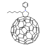
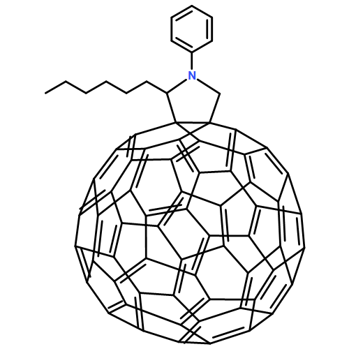
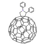

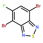


![4H-Silolo[3,2-b:4,5-b']dithiophene, 4,4-bis(2-ethylhexyl)-2-(trimethylstannyl)-](/data/chemimg/164900/1228237-08-8.png)
![4H-Silolo[3,2-b:4,5-b']dithiophene, 4,4-bis(2-ethylhexyl)-2-(trimethylstannyl)-](/data/chemimg/164900/1228237-08-8_b.png)
![4H-Silolo[3,2-b:4,5-b']dithiophene, 4,4-bis(2-ethylhexyl)-](/data/chemimg/164900/1207627-85-7.png)
![4H-Silolo[3,2-b:4,5-b']dithiophene, 4,4-bis(2-ethylhexyl)-](/data/chemimg/164900/1207627-85-7_b.png)
![BENZO[13,14]PENTAPHENO[3,4,5-DEF:10,9,8-D'E'F']DIISOQUINOLINE-1,3,10,12(2H,11H)-TETRONE, 2,11-BIS(1-HEPTYLOCTYL)-](http://img.cochemist.com/ccimg/881900/881877-80-1.png)
![BENZO[13,14]PENTAPHENO[3,4,5-DEF:10,9,8-D'E'F']DIISOQUINOLINE-1,3,10,12(2H,11H)-TETRONE, 2,11-BIS(1-HEPTYLOCTYL)-](http://img.cochemist.com/ccimg/881900/881877-80-1_b.png)
![Poly[bis(3-dodecyl-2-thienyl)-2,2'-dithiophene-5,5'-diyl]](http://img.cochemist.com/ccimg/827400/827343-06-6.png)
![Poly[bis(3-dodecyl-2-thienyl)-2,2'-dithiophene-5,5'-diyl]](http://img.cochemist.com/ccimg/827400/827343-06-6_b.png)


![Poly[[2,2'-bithiophene]-5,5'-diyl(9,9-dioctyl-9H-fluorene-2,7-diyl)]](http://img.cochemist.com/ccimg/210400/210347-56-1.png)
![Poly[[2,2'-bithiophene]-5,5'-diyl(9,9-dioctyl-9H-fluorene-2,7-diyl)]](http://img.cochemist.com/ccimg/210400/210347-56-1_b.png)


![Anthra[2,1,9-def:6,5,10-d'e'f']diisoquinoline-1,3,8,10(2H,9H)-tetrone, 2,9-dioctyl-](/data/chemimg/709500/78151-58-3.png)
![Anthra[2,1,9-def:6,5,10-d'e'f']diisoquinoline-1,3,8,10(2H,9H)-tetrone, 2,9-dioctyl-](/data/chemimg/709500/78151-58-3_b.png)


![Benzo[lmn][3,8]phenanthroline-1,3,6,8(2H,7H)-tetrone, 4,9-dibromo-2,7-bis(2-hexyldecyl)-](/data/chemimg/3730400/1459168-68-3.png)
![Benzo[lmn][3,8]phenanthroline-1,3,6,8(2H,7H)-tetrone, 4,9-dibromo-2,7-bis(2-hexyldecyl)-](/data/chemimg/3730400/1459168-68-3_b.png)
![Benzo[lmn][3,8]phenanthroline-1,3,6,8(2H,7H)-tetrone, 4,9-dibromo-2,7-bis(2-octyldodecyl)-](/data/chemimg/139000/1100243-35-3.png)
![Benzo[lmn][3,8]phenanthroline-1,3,6,8(2H,7H)-tetrone, 4,9-dibromo-2,7-bis(2-octyldodecyl)-](/data/chemimg/139000/1100243-35-3_b.png)
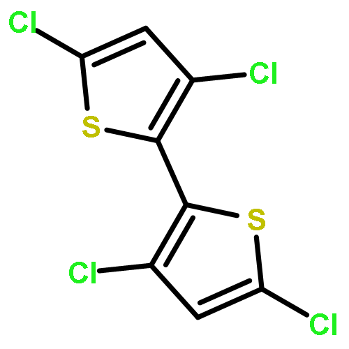


![Poly[(9,9-dioctylfluorenyl-2,7-diyl)-alt-(benzo[2,1,3]thiadiazol-4,7-diyl)]](/data/chemimg/107700/210347-52-7.png)
![Poly[(9,9-dioctylfluorenyl-2,7-diyl)-alt-(benzo[2,1,3]thiadiazol-4,7-diyl)]](/data/chemimg/107700/210347-52-7_b.png)


