Co-reporter:Qiqi Xu, Jianwen Zhao, Vincenzo Pecunia, Wenya Xu, Chunshan Zhou, Junyan Dou, Weibing Gu, Jian Lin, Lixin Mo, Yanfei Zhao, and Zheng Cui
ACS Applied Materials & Interfaces April 12, 2017 Volume 9(Issue 14) pp:12750-12750
Publication Date(Web):March 24, 2017
DOI:10.1021/acsami.7b01666
The fabrication of printed high-performance and environmentally stable n-type single-walled carbon nanotube (SWCNT) transistors and their integration into complementary (i.e., complementary metal–oxide–semiconductor, CMOS) circuits are widely recognized as key to achieving the full potential of carbon nanotube electronics. Here, we report a simple, efficient, and robust method to convert the polarity of SWCNT thin-film transistors (TFTs) using cheap and readily available ethanolamine as an electron doping agent. Printed p-type bottom-gate SWCNT TFTs can be selectively converted into n-type by deposition of ethanolamine inks on the transistor active region via aerosol jet printing. Resulted n-type TFTs show excellent electrical properties with an on/off ratio of 106, effective mobility up to 30 cm2 V–1 s–1, small hysteresis, and small subthreshold swing (90–140 mV dec–1), which are superior compared to the original p-type SWCNT devices. The n-type SWCNT TFTs also show good stability in air, and any deterioration of performance due to shelf storage can be fully recovered by a short low-temperature annealing. The easy polarity conversion process allows construction of CMOS circuitry. As an example, CMOS inverters were fabricated using printed p-type and n-type TFTs and exhibited a large noise margin (50 and 103% of 1/2 Vdd = 1 V) and a voltage gain as high as 30 (at Vdd = 1 V). Additionally, the CMOS inverters show full rail-to-rail output voltage swing and low power dissipation (0.1 μW at Vdd = 1 V). The new method paves the way to construct fully functional complex CMOS circuitry by printed TFTs.Keywords: ethanolamine; n-type and p-type; printed CMOS inverters; printed thin film transistors; selective polarity conversion; sorted semiconducting carbon nanotube;
Co-reporter:Wei Gao;Junkai Wang;Qun Luo;Yi Lin;Yuchao Ma;Junyan Dou;Hongwei Tan;Chang-Qi Ma
RSC Advances (2011-Present) 2017 vol. 7(Issue 3) pp:1606-1616
Publication Date(Web):2017/01/04
DOI:10.1039/C6RA25567A
Three-dimensional (3D) π-conjugated dendrimers are a new class of structurally defined macromolecules for use in organic electronics. Herein, a new family of dendritic oligothiophenes (DOT-c-BTs) up to the 2nd generation with benzothiadiazole (BT) groups at the core have been synthesized by a precise convergent approach. The well-defined chemical structures and the monodispersed nature of these DOT-c-BTs were fully confirmed by NMR spectroscopy, MALDI-TOF mass spectrometry (MALDI-TOF MS), high-resolution mass spectrometry (HR MS), and gel-permeation chromatography (GPC) measurements. The optical and electrochemical properties were investigated by UV-vis absorption, and cyclic voltammetry. The insertion of electron-deficient benzothiadiazole (BT) groups into the core of the conjugated dendritic oligothiophenes resulted in a large redshift compared to all-thiophene dendrimers. Cyclic voltammetry measurements showed one reversible reduction process and multiple oxidation waves for these functionalized dendritic oligothiophenes, due to the reduction of the BT core and the oxidation of different π-conjugated chains, respectively. Applications of DOT-c-BTs in organic solar cells as the electron donor were presented. However, unfavorable nanophase separation in the blended film led to poor device performance.
Co-reporter:Wenya Xu, Junyan Dou, Jianwen Zhao, Hongwei Tan, Jun Ye, Masayoshi Tange, Wei Gao, Weiwei Xu, Xiang Zhang, Wenrui Guo, Changqi Ma, Toshiya Okazaki, Kai Zhang and Zheng Cui
Nanoscale 2016 vol. 8(Issue 8) pp:4588-4598
Publication Date(Web):26 Jan 2016
DOI:10.1039/C6NR00015K
Two innovative research studies are reported in this paper. One is the sorting of semiconducting carbon nanotubes and ink formulation by a novel semiconductor copolymer and second is the development of CMOS inverters using not the p-type and n-type transistors but a printed p-type transistor and a printed ambipolar transistor. A new semiconducting copolymer (named P-DPPb5T) was designed and synthesized with a special nonlinear structure and more condensed conjugation surfaces, which can separate large diameter semiconducting single-walled carbon nanotubes (sc-SWCNTs) from arc discharge SWCNTs according to their chiralities with high selectivity. With the sorted sc-SWCNTs ink, thin film transistors (TFTs) have been fabricated by aerosol jet printing. The TFTs displayed good uniformity, low operating voltage (±2 V) and subthreshold swing (SS) (122–161 mV dec−1), high effective mobility (up to 17.6–37.7 cm2 V−1 s−1) and high on/off ratio (104–107). With the printed TFTs, a CMOS inverter was constructed, which is based on the p-type TFT and ambipolar TFT instead of the conventional p-type and n-type TFTs. Compared with other recently reported inverters fabricated by printing, the printed CMOS inverters demonstrated a better noise margin (74% 1/2 Vdd) and was hysteresis free. The inverter has a voltage gain of up to 16 at an applied voltage of only 1 V and low static power consumption.
Co-reporter:Chunshan Zhou, Jianwen Zhao, Jun Ye, Masayoshi Tange, Xiang Zhang, Weiwei Xu, Kedong Zhang, Toshiya Okazaki, Zheng Cui
Carbon 2016 108() pp: 372-380
Publication Date(Web):1 November 2016
DOI:10.1016/j.carbon.2016.07.035
In this work, a new poly(9,9-dioctylfluorene) (PFO) derivative (named PFIID) with the large conjugated planar surfaces was designed and synthesized, and the ability to sort sc-SWCNTs was investigated in detailed. The absorption spectra of sorted SWCNT solutions demonstrated that PFIID exhibited the ability to selectively and efficiently sort sc-SWCNTs from commercial arc discharge carbon nanotubes. The underlying separation mechanism was studied with the aid of photoluminescence excitation (PLE) spectra and the molecular dynamic simulation. It was found that the simulation results agreed well with the experimental data. PFIID-sorted sc-SWCNTs were acted as the channel materials to construct printed thin-film transistors (TFTs) and nitrogen dioxide gas sensors. Printed SWCNT TFTs exhibited superior performance with good uniformity, high on/off ratios (∼106), high effective hole mobility (∼29.8 cm2 V−1 s−1) and small subthreshold swing (SS) (142–163 mV/dec) at low operating voltage (±2 V). NO2 gas sensors also showed good performance with high sensitivity (ΔR/Ro∼96%), fast response (30 s), good stability and the recovery time of 30 s when exposed to 60 ppm NO2 at room temperature. Both of the sensitivity and recovery time are one of the best performances reported for NO2 gas sensors at room temperature.
Co-reporter:Zheng Chen, Xichao Qin, Teng Zhou, Xinzhou Wu, Shuangshuang Shao, Meilan Xie and Zheng Cui
Journal of Materials Chemistry A 2015 vol. 3(Issue 43) pp:11464-11470
Publication Date(Web):06 Oct 2015
DOI:10.1039/C5TC00180C
Highly conductive indium tin oxide (ITO) nanocrystals and inks have been synthesized by solvothermal dehydration condensation of metal hydroxide in combination with in situ ethanolamine capping. It is found that the addition of ethanolamine can effectively reduce the size of nanocrystals and chemically modify their surfaces. The synthesized ITO nanocrystals can be well dispersed in ethanol with high solid content and the suspension is stable for days. Such a small-molecule capped ITO suspension has been used as a conductive ink to make transparent conductive films by spin coating. Furthermore, a water washing step has been introduced in the ITO film preparation process to improve their conductivity, resulting in a low resistivity of 8.9 × 10⁻³ Ω cm after 2 hour annealing at 300 °C in a mixed Ar and H2 atmosphere.
Co-reporter:Jinyong Zhuang, Wanfei Li, Weichen Wu, Minshun Song, Wenming Su, Ming Zhou and Zheng Cui
New Journal of Chemistry 2015 vol. 39(Issue 1) pp:246-253
Publication Date(Web):28 Oct 2014
DOI:10.1039/C4NJ01316F
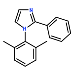
As an extension of our previous study, three sky-blue homoleptic iridium(III) complexes 1–3 with fluorine-free phenylimidazole ligands were synthesized and their photophysical, electrochemical and thermal properties were studied. All the complexes showed high photoluminescence quantum yields ranging from 0.50 to 0.53. The introduction of a bulky isopropyl group at the 2,6-position of N-phenyl of the phenylimidazole ligands increases the quantum yield and the decomposition temperature of the iridium(III) complexes. As the conjugated system of the ligand becomes larger, a very small bathochromic-shift of 1 nm was observed in complex 3 (475 nm) compared with complexes 1 (474 nm) and 2 (474 nm). All the OLED devices showed high current efficiencies of over 20 cd A−1 at the luminance of 1000 cd m−2. Devices incorporated with complexes 1–3 all showed longer lifetime in comparison with that of a FIrpic-based device.
Co-reporter:Xinzhou Wu, Zheng Chen, Teng Zhou, Shuangshuang Shao, Meilan Xie, Mingshun Song and Zheng Cui
RSC Advances 2015 vol. 5(Issue 27) pp:20924-20930
Publication Date(Web):05 Feb 2015
DOI:10.1039/C4RA17234E
Thermally cross-linkable poly(methylsilsesquioxane) (PMSQ) has been investigated as a printable dielectric ink to make the gate insulator for solution processed metal oxide (IGZO) thin-film transistors by aerosol jet printing. It was found that by increasing the curing temperature from 150 to 200 °C, the dielectric constant and loss tangent of the printed PMSQ layer reduces dramatically. The mobility, leakage current and gate current of the PMSQ enabled thin-film transistor reduces accordingly, while the on/off ratio increases with the increase of curing temperature. An interfacial layer was introduced to further improve the on/off ratio to 3 × 10⁵ and reduce the leakage current to 2.6 × 10⁻¹⁰ A, which is the best result for the solution processed IGZO thin-film transistors using the PMSQ as the gate insulator at a curing temperature of only 150 °C. The study has demonstrated the feasibility of fabricating IGZO thin-film transistors by an all solution-based process.
Co-reporter:Fei Fei, Jinyong Zhuang, Weichen Wu, Minshun Song, Dongyu Zhang, Sen Li, Wenming Su and Zheng Cui
RSC Advances 2015 vol. 5(Issue 1) pp:608-611
Publication Date(Web):18 Nov 2014
DOI:10.1039/C4RA09197C
A printed aluminum cathode with low sintering temperature has been achieved using an aluminum precursor ink, AlH3·O(C3H7)2, which in the presence of a TiCl4 catalyst can be printed to give the required pattern and then sintered at 80 °C for 30 s to form an Al film. The Al cathode of 50 nm thickness has a sheet resistance of 2.09 Ω □−1 and work function of 3.67 eV. The study demonstrates that the low sintering temperature and work function of the printed film, together with its high conductivity and stability, mean that it is well suited for use as an OLED cathode and that it paves the way for fully printed flexible devices.
Co-reporter:Weiwei Xu, Zhen Liu, Jianwen Zhao, Wenya Xu, Weibing Gu, Xiang Zhang, Long Qian and Zheng Cui
Nanoscale 2014 vol. 6(Issue 24) pp:14891-14897
Publication Date(Web):13 Oct 2014
DOI:10.1039/C4NR05471G
In this report printed thin film transistors and logic circuits on flexible substrates are reported. The top-gate thin film transistors were made of the sorted semiconducting single-walled carbon nanotubes (sc-SWCNTs) ink as channel material and printed silver lines as top electrodes and interconnect. 5 nm HfOx thin films pre-deposited on PET substrates by atomic layer deposition (ALD) act as the adhesion layers to significantly improve the immobilization efficiency of sc-SWCNTs and environmental stability. The immobilization mechanism was investigated in detail. The flexible partially-printed top-gate SWCNT TFTs display ambipolar characteristics with slightly strong p-type when using 50 nm HfOx thin films as dielectric layer, as well as the encapsulation layer by atomic layer deposition (ALD) at 120 °C. The hole mobility, on/off ratio and subthreshold swing (SS) are ∼46.2 cm2 V−1 s−1, 105 and 109 mV per decade, respectively. Furthermore, partially-printed TFTs show small hysteresis, low operating voltage (2 V) and high stability in air. Flexible partially-printed inverters show good performance with voltage gain up to 33 with 1.25 V supply voltage, and can work at 10 kHz. The frequency of flexible partially-printed five-stage ring oscillators can reach 1.7 kHz at supply voltages of 2 V with per stage delay times of 58.8 μs. This work paves a way to achieve printed SWCNT advanced logic circuits and systems on flexible substrates.
Co-reporter:Zhen Liu, Jianwen Zhao, Wenya Xu, Long Qian, Shuhong Nie, and Zheng Cui
ACS Applied Materials & Interfaces 2014 Volume 6(Issue 13) pp:9997
Publication Date(Web):June 16, 2014
DOI:10.1021/am502168x
The precise placement and efficient deposition of semiconducting single-walled carbon nanotubes (sc-SWCNTs) on substrates are challenges for achieving printed high-performance SWCNT thin-film transistors (TFTs) with independent gates. It was found that the wettability of the substrate played a key role in the electrical properties of TFTs for sc-SWCNTs sorted by poly[(9,9-dioctylfluorene-2,7-diyl)-co-(1,4-benzo-2,1,3-thiadiazole)] (PFO-BT). In the present work we report a simple and scalable method which can rapidly and selectively deposit a high concentration of sc-SWCNTs in TFT channels by aerosol-jet-printing. The method is based on oxygen plasma treatment of substrates, which tunes the surface wettability. TFTs printed on the treated substrates demonstrated a low operation voltage, small hysteresis, high mobility up to 32.3 cm2 V–1 s–1, and high on/off ratio up to 106 after only two printings. Their mobilities were 10 and 30 times higher than those of TFTs fabricated on untreated and low-wettability substrates. The uniformity of printed TFTs was also greatly improved. Inverters were constructed by printed top-gate TFTs, and a maximum voltage gain of 17 at Vdd = 5 V was achieved. The mechanism of such improvements is that the PFO-BT-functionalized sc-SWCNTs are preferably immobilized on the oxygen plasma treated substrates due to the strong hydrogen bonds between sc-SWCNTs and hydroxyl groups on the substrates.Keywords: electrical properties; printed thin-film transistors; single-walled carbon nanotube; sorted; uniformity; wettability
Co-reporter:Xinzhou Wu, Fei Fei, Zheng Chen, Wenming Su, Zheng Cui
Composites Science and Technology 2014 Volume 94() pp:117-122
Publication Date(Web):9 April 2014
DOI:10.1016/j.compscitech.2014.01.024
A new nanocomposite dielectric ink has been developed by dispersing Ca2Nb3O10 nanosheets in acetone diluted PMMA solution. Dielectric films were formed by printing the ink with an aerosol jet printer. SEM images showed that the 2D nanosheets were homogeneously distributed in the printed films which exhibited higher dielectric constants than PMMA, low dielectric loss and good dielectric stability over a wide range of frequencies. The effect of nanosheet content in the ink has been investigated. Thin-film transistors based on indium gallium zinc oxide semiconductor material were fabricated with the printed nanocomposite insulator. The feasibility of printing dielectrics based on the new nanocomposite ink for thin-film transistors has been demonstrated.
Co-reporter:Jinyong Zhuang, Wanfei Li, Wenming Su, Ming Zhou and Zheng Cui
New Journal of Chemistry 2014 vol. 38(Issue 2) pp:650-656
Publication Date(Web):11 Dec 2013
DOI:10.1039/C3NJ01054F
A novel bipolar host material 9-(3-(5-(4-(diphenylphosphoryl)phenyl)-4-phenyl-4H-1,2,4-triazol-3-yl)phenyl)-9H-carbazole (CTPO) with carbazole, triazole and phosphine oxide moieties was designed and synthesized. CTPO was found to exhibit a high glass transition temperature (Tg = 127 °C), suitable HOMO and LUMO levels (5.65 and 2.42 eV), a high triplet energy (3.06 eV) and excellent bipolar properties. A device with 15 wt% doping concentration showed a low turn-on voltage of 2.5 V and maximum current and power efficiencies of 41.6 cd A−1 and 43.0 lm W−1, respectively. A high efficiency of 40.1 cd A−1 was achieved at the brightness of 100 cd m−2. Even at a high luminance of 1000 cd m−2, the efficiency remained as high as 35.2 cd A−1.
Co-reporter:Chao Wang;Wenya Xu;Jianwen Zhao;Jian Lin;Zheng Chen
Journal of Materials Science 2014 Volume 49( Issue 5) pp:2054-2062
Publication Date(Web):2014 March
DOI:10.1007/s10853-013-7895-3
A simple and scalable method has been developed to preferentially eliminate metallic species in several commercial single-walled carbon nanotubes (SWCNTs), such as CoMoCAT 65, CoMoCAT 76, CG 200, HiPco, and arc discharge (P2) SWCNTs, using 4-nitrobenzenediazonium salts by tuning the types and concentrations of surfactants in aqueous solutions. The selectivity in commonly used surfactant solutions was confirmed by ultra violet-visible-near infrared spectra, Raman spectra and electrical characterization. Good-performance printed thin-film transistors (TFTs) were obtained by inkjet printing. The printed TFTs exhibited excellent electrical properties with effective mobility and on/off ratio upto 3.54 cm2 V−1 s−1 and 3 × 10⁵, respectively. This method does not require complicated reaction conditions and tedious purification procedure, therefore, promises low-cost production of high-performance printed TFT devices for electronic applications.
Co-reporter:Chao Wang, Long Qian, Wenya Xu, Shuhong Nie, Weibing Gu, Jianhui Zhang, Jianwen Zhao, Jian Lin, Zheng Chen and Zheng Cui
Nanoscale 2013 vol. 5(Issue 10) pp:4156-4161
Publication Date(Web):02 Apr 2013
DOI:10.1039/C3NR34304A
In this work, a simple and rapid method to selectively sort semiconducting-SWCNTs (sc-SWCNTs) with large diameters using regioregular poly(3-dodecylthiophene) (rr-P3DDT) is presented. The absorption spectra and Raman spectra demonstrated that metallic species of arc discharge SWCNTs were effectively removed after interaction with rr-P3DDT in toluene with the aid of sonication and centrifugation. The sorted sc-SWCNT inks have been directly used to fabricate thin film transistors (TFTs) by dip-coating, drop-casting and inkjet printing. TFTs with an effective mobility of ∼34 cm2 V−1 s−1 and on–off ratios of ∼107 have been achieved by dip coating and drop casting the ink on SiO2/Si substrates with pre-patterned interdigitated gold electrode arrays. The printed devices also showed excellent electrical properties with a mobility of up to 6.6 cm2 V−1 s−1 and on–off ratios of up to 105. Printed inverters based on the TFTs have been constructed on glass substrates, showing a maximum voltage gain of 112 at a Vdd of −5 V. This work paves the way for making printable logic circuits for real applications.
Co-reporter:Xinzhou Wu, Zheng Chen, Zheng Cui
Composites Science and Technology 2013 Volume 81() pp:48-53
Publication Date(Web):14 June 2013
DOI:10.1016/j.compscitech.2013.03.021
Albumen and BaTiO3 nanoparticles are employed to make solution processable nanocomposite for high permittivity films. The nanoparticles are modified with poly(acrylic acid) molecules to achieve homogeneous dispersion in albumen aqueous solution and made into films by drop casting. The dielectric constant and loss tangent of albumen–BaTiO3 nanocomposites are investigated as the function of volume fraction of BaTiO3. The nanocomposites exhibit maximum relative permittivity of 52 and good dielectric stability over a wide range of frequency, while the loss tangent is below 0.05 even at high BaTiO3 loading of 80 vol%. The dielectric constants of nanocomposites with lower volume fractions (<41 vol%) are in good agreement with the Lichtenecker-Logarithmic model.
Co-reporter:Long Qian, Wenya Xu, XiaoFeng Fan, Chao Wang, Jianhui Zhang, Jianwen Zhao, and Zheng Cui
The Journal of Physical Chemistry C 2013 Volume 117(Issue 35) pp:18243-18250
Publication Date(Web):August 8, 2013
DOI:10.1021/jp4055022
In this work, a simple and effective method has been developed to selectively separate large-diameter semiconducting-SWCNTs (sc-SWCNTs) from commercial arc discharge SWCNTs using (9,9-dioctylfluorene-co-bithiophene) (F8T2). The role of solvents in the separation and dispersion processes was studied. It has been proved that sc-SWCNTs mixed in arc discharge SWCNTs can be selectively sorted by F8T2 in toluene, xylene, or m-xylene with the aid of sonication and centrifugation, and the molecular dynamic simulation also agrees with the experiment results. The resulted sc-SWCNTs dispersion solution was used as a printable ink to print thin-film transistors (TFTs) via an aerosol jet printer. The printed TFTs showed good uniformity and electrical properties with on current up to 10–3 A, effective mobility up to 42.1 cm2 V–1 s–1 (±1.2 cm2 V–1 s–1), and on/off ratio of ∼107 after only four cycles of repeated printing. In addition, all of the printed devices exhibited rapid photocurrent response to light irradiation.
Co-reporter:Jianwen Zhao, Yulong Gao, Weibing Gu, Chao Wang, Jian Lin, Zheng Chen and Zheng Cui
Journal of Materials Chemistry A 2012 vol. 22(Issue 38) pp:20747-20753
Publication Date(Web):16 Aug 2012
DOI:10.1039/C2JM34598F
In this manuscript, we developed a high-performance, printable and water-based semiconducting SCNT ink, and fabricated all-printed chemically functionalized CoMoCat 76 SCNT thin film transistors (TFTs) on flexible substrates via a suite of printing technologies. The metallic species in the pristine CoMoCat 76 SCNTs were effectively eliminated by organic radicals, and the functionalized SCNTs were characterized by UV-Vis-NIR spectroscopy and Raman spectra. The high quality, printable and water-based functionalized SCNT inks were obtained by tuning the ink ingredients, such as the concentrations of surfactants and additives. The printing methods we investigated include inkjet printing, aerosol jet printing and a hybrid with nanoimprinting. Large area source and drain electrode patterns were first fabricated on flexible substrates by a hybrid printing method, and then the optimal SCNT ink was printed on the channel of the TFT devices by ink-jet printing. Subsequently, the silver side-gate electrode and ion gel dielectric layer were deposited by aerosol jet printing. The all-printed flexible TFTs exhibited an effective mobility up to 1.5 cm2 V−1 s−1 and an on/off ratio up to 4 × 10³. This work opens up a way to fabricate scalable and all-printed flexible electronics, and it is of benefit to generalize the practical applications of flexible electronics in the future.
Co-reporter:Jianwen Zhao, Yulong Gao, Jian Lin, Zheng Chen and Zheng Cui
Journal of Materials Chemistry A 2012 vol. 22(Issue 5) pp:2051-2056
Publication Date(Web):12 Dec 2011
DOI:10.1039/C1JM14773K
A simple and scalable method to print high performance thin-film transistors (TFTs) with high yield by an aerosol jet printer has been developed, using water-based and chemically functionalized single-walled carbon nanotube (SCNT) inks as the semiconducting layer. The absorption spectra, Raman spectra and photoluminescence excitation (PLE) spectra of the SCNT ink indicated that metallic species and small diameter semiconducting species in CoMoCat 76 were effectively eliminated after reaction with 2,2-azobisisobutyronitrile (AIBN) in dimethyformamide (DMF). The functionalized SCNTs were dispersed in 1% SDS aqueous solution, and the as-prepared SCNTs inks were directly used to print TFTs using an aerosol jet printing system without any additional purification. Printed TFTs with high yield were obtained by tuning the concentrations of SCNTs and surfactants in the inks. The printed side-gate and bottom-gate TFTs exhibited the effective mobility of ∼1 cm2 V−1 s−1 and an on/off ratio over 103. In addition, these printed TFTs were hysteresis-free and able to operate at low-voltage when using printable high-capacitance ion gel as the dielectric layer. The new method has opened the route to fabricate all-printed SCNT TFTs on flexible substrate with high performance.
Co-reporter:Jianwen Zhao, Yulong Gao, Weibing Gu, Chao Wang, Jian Lin, Zheng Chen and Zheng Cui
Journal of Materials Chemistry A 2012 - vol. 22(Issue 38) pp:NaN20753-20753
Publication Date(Web):2012/08/16
DOI:10.1039/C2JM34598F
In this manuscript, we developed a high-performance, printable and water-based semiconducting SCNT ink, and fabricated all-printed chemically functionalized CoMoCat 76 SCNT thin film transistors (TFTs) on flexible substrates via a suite of printing technologies. The metallic species in the pristine CoMoCat 76 SCNTs were effectively eliminated by organic radicals, and the functionalized SCNTs were characterized by UV-Vis-NIR spectroscopy and Raman spectra. The high quality, printable and water-based functionalized SCNT inks were obtained by tuning the ink ingredients, such as the concentrations of surfactants and additives. The printing methods we investigated include inkjet printing, aerosol jet printing and a hybrid with nanoimprinting. Large area source and drain electrode patterns were first fabricated on flexible substrates by a hybrid printing method, and then the optimal SCNT ink was printed on the channel of the TFT devices by ink-jet printing. Subsequently, the silver side-gate electrode and ion gel dielectric layer were deposited by aerosol jet printing. The all-printed flexible TFTs exhibited an effective mobility up to 1.5 cm2 V−1 s−1 and an on/off ratio up to 4 × 10³. This work opens up a way to fabricate scalable and all-printed flexible electronics, and it is of benefit to generalize the practical applications of flexible electronics in the future.
Co-reporter:Jianwen Zhao, Yulong Gao, Jian Lin, Zheng Chen and Zheng Cui
Journal of Materials Chemistry A 2012 - vol. 22(Issue 5) pp:NaN2056-2056
Publication Date(Web):2011/12/12
DOI:10.1039/C1JM14773K
A simple and scalable method to print high performance thin-film transistors (TFTs) with high yield by an aerosol jet printer has been developed, using water-based and chemically functionalized single-walled carbon nanotube (SCNT) inks as the semiconducting layer. The absorption spectra, Raman spectra and photoluminescence excitation (PLE) spectra of the SCNT ink indicated that metallic species and small diameter semiconducting species in CoMoCat 76 were effectively eliminated after reaction with 2,2-azobisisobutyronitrile (AIBN) in dimethyformamide (DMF). The functionalized SCNTs were dispersed in 1% SDS aqueous solution, and the as-prepared SCNTs inks were directly used to print TFTs using an aerosol jet printing system without any additional purification. Printed TFTs with high yield were obtained by tuning the concentrations of SCNTs and surfactants in the inks. The printed side-gate and bottom-gate TFTs exhibited the effective mobility of ∼1 cm2 V−1 s−1 and an on/off ratio over 103. In addition, these printed TFTs were hysteresis-free and able to operate at low-voltage when using printable high-capacitance ion gel as the dielectric layer. The new method has opened the route to fabricate all-printed SCNT TFTs on flexible substrate with high performance.
Co-reporter:Zheng Chen, Xichao Qin, Teng Zhou, Xinzhou Wu, Shuangshuang Shao, Meilan Xie and Zheng Cui
Journal of Materials Chemistry A 2015 - vol. 3(Issue 43) pp:NaN11470-11470
Publication Date(Web):2015/10/06
DOI:10.1039/C5TC00180C
Highly conductive indium tin oxide (ITO) nanocrystals and inks have been synthesized by solvothermal dehydration condensation of metal hydroxide in combination with in situ ethanolamine capping. It is found that the addition of ethanolamine can effectively reduce the size of nanocrystals and chemically modify their surfaces. The synthesized ITO nanocrystals can be well dispersed in ethanol with high solid content and the suspension is stable for days. Such a small-molecule capped ITO suspension has been used as a conductive ink to make transparent conductive films by spin coating. Furthermore, a water washing step has been introduced in the ITO film preparation process to improve their conductivity, resulting in a low resistivity of 8.9 × 10⁻³ Ω cm after 2 hour annealing at 300 °C in a mixed Ar and H2 atmosphere.


![Poly[(9,9-dioctylfluorenyl-2,7-diyl)-alt-(benzo[2,1,3]thiadiazol-4,7-diyl)]](/data/chemimg/107700/210347-52-7.png)
![Poly[(9,9-dioctylfluorenyl-2,7-diyl)-alt-(benzo[2,1,3]thiadiazol-4,7-diyl)]](/data/chemimg/107700/210347-52-7_b.png)